JAJSMY4C September   2021  – December 2022 UCC14240-Q1

PRODUCTION DATA  

  1. 特長
  2. アプリケーション
  3. 概要
  4. Revision History
  5. Pin Configuration and Functions
  6. Specifications
    1. 6.1  Absolute Maximum Ratings
    2. 6.2  ESD Ratings
    3. 6.3  Recommended Operating Conditions
    4. 6.4  Thermal Information
    5. 6.5  Power Ratings
    6. 6.6  Insulation Specifications
    7. 6.7  Safety-Related Certifications
    8. 6.8  Electrical Characteristics
    9. 6.9  Safety Limiting Values
    10. 6.10 Insulation Characteristics
    11. 6.11 Typical Characteristics
  7. Detailed Description
    1. 7.1 Overview
    2. 7.2 Functional Block Diagram
    3. 7.3 Feature Description
      1. 7.3.1 Power Stage Operation
        1. 7.3.1.1 VDD-VEE Voltage Regulation
        2. 7.3.1.2 COM-VEE Voltage Regulation
        3. 7.3.1.3 Power Handling Capability
      2. 7.3.2 Output Voltage Soft Start
      3. 7.3.3 ENA and PG
      4. 7.3.4 Protection Functions
        1. 7.3.4.1 Input Undervoltage Lockout
        2. 7.3.4.2 Input Overvoltage Lockout
        3. 7.3.4.3 Output Overvoltage Protection
        4. 7.3.4.4 Overpower Protection
          1. 7.3.4.4.1 Output Undervoltage Protection
        5. 7.3.4.5 Overtemperature Protection
    4. 7.4 Device Functional Modes
  8. Application and Implementation
    1. 8.1 Application Information
    2. 8.2 Typical Application
      1. 8.2.1 Design Requirements
      2. 8.2.2 Detailed Design Procedure
        1. 8.2.2.1 Capacitor Selection
        2. 8.2.2.2 RLIM Resistor Selection
      3. 8.2.3 Application Curves
    3. 8.3 System Examples
    4. 8.4 Power Supply Recommendations
    5. 8.5 Layout
      1. 8.5.1 Layout Guidelines
      2. 8.5.2 Layout Example
  9. Device and Documentation Support
    1. 9.1 Documentation Support
      1. 9.1.1 Related Documentation
    2. 9.2 ドキュメントの更新通知を受け取る方法
    3. 9.3 サポート・リソース
    4. 9.4 Trademarks
    5. 9.5 静電気放電に関する注意事項
    6. 9.6 用語集
  10. 10Mechanical, Packaging, and Orderable Information

パッケージ・オプション

メカニカル・データ(パッケージ|ピン)
サーマルパッド・メカニカル・データ
発注情報

Layout Example

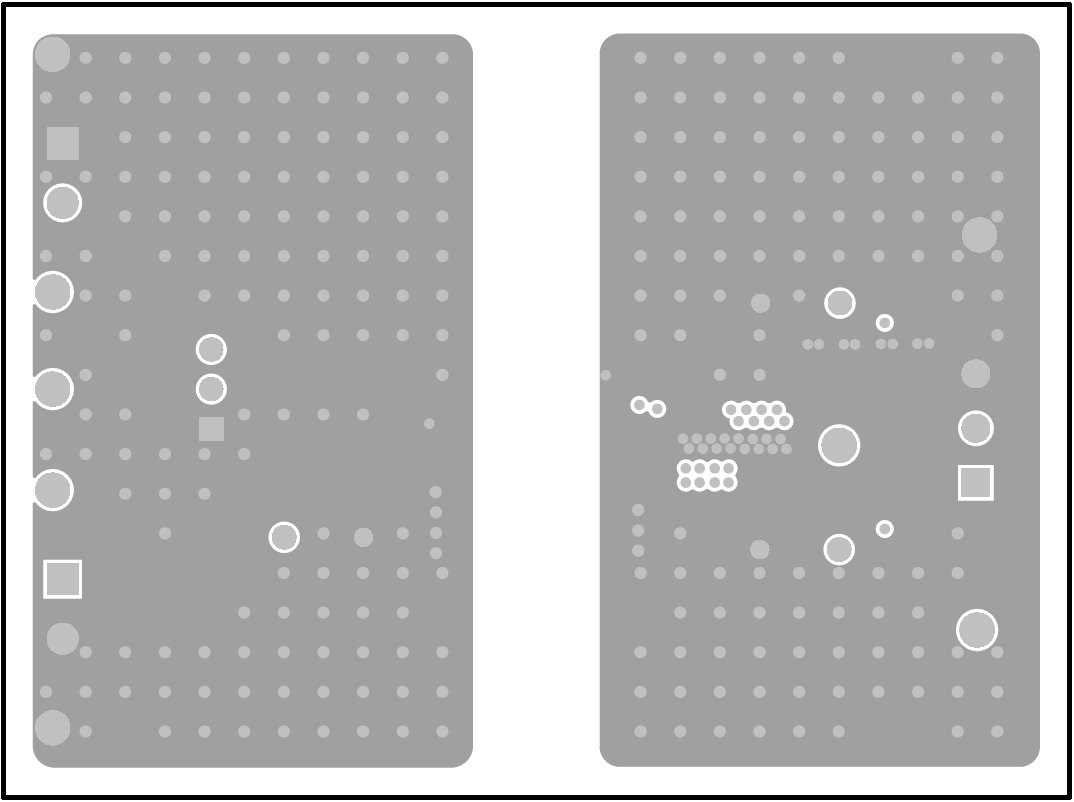
The layout example shown in the following figures is from the evaluation board UCC14240-Q1EVM, UCC14240EVM-052, and based on the Figure 8-1 design.


GUID-20221121-SS0I-QD9J-Z55K-BPFWCTGPR91D-low.png

Figure 8-13 UCC14240-Q1EVM, PCB Top Layer, Assembly

GUID-20221121-SS0I-SPHK-3NXC-8SXGGNSGMLGX-low.png

Figure 8-14 UCC14240-Q1EVM, Signal Layer 2 (Same as Layer 3)
GUID-20221121-SS0I-BDXM-9NFT-4LKS3CJMLFVL-low.png

Figure 8-15 UCC14240-Q1EVM, Signal Layer 3 (Same as Layer 2)

GUID-20221121-SS0I-9GF5-9HXP-PRWTPWRF4XWK-low.png

Figure 8-16 UCC14240-Q1EVM, PCB Bottom Layer, Assembly (Mirrored View)