JAJSE88G November 2017 – November 2024 UCC21220 , UCC21220A
PRODUCTION DATA
- 1
- 1 特長
- 2 アプリケーション
- 3 概要
- 4 Device Comparison Table
- 5 Pin Configuration and Functions
- 6 Specifications
- 7 Parameter Measurement Information
- 8 Detailed Description
-
9 Application and Implementation
- 9.1 Application Information
- 9.2
Typical Application
- 9.2.1 Design Requirements
- 9.2.2
Detailed Design Procedure
- 9.2.2.1 Designing INA/INB Input Filter
- 9.2.2.2 Select External Bootstrap Diode and its Series Resistor
- 9.2.2.3 Gate Driver Output Resistor
- 9.2.2.4 Estimating Gate Driver Power Loss
- 9.2.2.5 Estimating Junction Temperature
- 9.2.2.6 Selecting VCCI, VDDA/B Capacitor
- 9.2.2.7 Application Circuits with Output Stage Negative Bias
- 9.2.3 Application Curves
- 10Power Supply Recommendations
- 11Layout
- 12Device and Documentation Support
- 13Revision History
- 14Mechanical, Packaging, and Orderable Information
パッケージ・オプション
デバイスごとのパッケージ図は、PDF版データシートをご参照ください。
メカニカル・データ(パッケージ|ピン)
- D|16
サーマルパッド・メカニカル・データ
発注情報
8.3.1 VDD, VCCI, and Under Voltage Lock Out (UVLO)
The UCC21220 and UCC21220A have an internal under voltage lock out (UVLO) protection feature on the supply circuit blocks between the VDD and VSS pins for both outputs. When the VDD bias voltage is lower than VVDD_ON at device start-up or lower than VVDD_OFF after start-up, the VDD UVLO feature holds the effected output low, regardless of the status of the input pins (INA and INB).
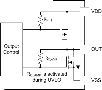
When the output stages of the driver are in an unbiased or UVLO condition, the driver outputs are held low by an active clamp circuit that limits the voltage rise on the driver outputs (Illustrated in Figure 8-1). In this condition, the upper PMOS is resistively held off by RHi-Z while the lower NMOS gate is tied to the driver output through RCLAMP. In this configuration, the output is effectively clamped to the threshold voltage of the lower NMOS device, typically around 1.5V, when no bias power is available.
 Figure 8-1 Simplified Representation of Active Pull Down Feature
The VDD UVLO protection has a hysteresis feature (VVDD_HYS). This hysteresis prevents chatter when there is ground noise from the power supply. Also this allows the device to accept small drops in bias voltage, which is bound to happen when the device starts switching and operating current consumption increases suddenly.
The input side of the UCC21220 and UCC21220A also have an internal under voltage lock out (UVLO) protection feature. The device isn't active unless the voltage, VCCI, is going to exceed VVCCI_ON on start up. And a signal will cease to be delivered when that pin receives a voltage less than VVCCI_OFF. And, just like the UVLO for VDD, there is hystersis (VVCCI_HYS) to ensure stable operation.
| CONDITION | INPUTS | OUTPUTS | ||
|---|---|---|---|---|
| INA | INB | OUTA | OUTB | |
| VCCI-GND < VVCCI_ON during device start up | H | L | L | L |
| VCCI-GND < VVCCI_ON during device start up | L | H | L | L |
| VCCI-GND < VVCCI_ON during device start up | H | H | L | L |
| VCCI-GND < VVCCI_ON during device start up | L | L | L | L |
| VCCI-GND < VVCCI_OFF after device start up | H | L | L | L |
| VCCI-GND < VVCCI_OFF after device start up | L | H | L | L |
| VCCI-GND < VVCCI_OFF after device start up | H | H | L | L |
| VCCI-GND < VVCCI_OFF after device start up | L | L | L | L |
| CONDITION | INPUTS | OUTPUTS | ||
|---|---|---|---|---|
| INA | INB | OUTA | OUTB | |
| VDD-VSS < VVDD_ON during device start up | H | L | L | L |
| VDD-VSS < VVDD_ON during device start up | L | H | L | L |
| VDD-VSS < VVDD_ON during device start up | H | H | L | L |
| VDD-VSS < VVDD_ON during device start up | L | L | L | L |
| VDD-VSS < VVDD_OFF after device start up | H | L | L | L |
| VDD-VSS < VVDD_OFF after device start up | L | H | L | L |
| VDD-VSS < VVDD_OFF after device start up | H | H | L | L |
| VDD-VSS < VVDD_OFF after device start up | L | L | L | L |