JAJSE88G November   2017  – November 2024 UCC21220 , UCC21220A

PRODUCTION DATA  

  1.   1
  2. 特長
  3. アプリケーション
  4. 概要
  5. Device Comparison Table
  6. Pin Configuration and Functions
  7. Specifications
    1. 6.1  Absolute Maximum Ratings
    2. 6.2  ESD Ratings
    3. 6.3  Recommended Operating Conditions
    4. 6.4  Thermal Information
    5. 6.5  Power Ratings
    6. 6.6  Insulation Specifications
    7. 6.7  Safety-Limiting Values
    8. 6.8  Electrical Characteristics
    9. 6.9  Switching Characteristics
    10. 6.10 Thermal Derating Curves
    11. 6.11 Typical Characteristics
  8. Parameter Measurement Information
    1. 7.1 Minimum Pulses
    2. 7.2 Propagation Delay and Pulse Width Distortion
    3. 7.3 Rising and Falling Time
    4. 7.4 Input and Disable Response Time
    5. 7.5 Power-up UVLO Delay to OUTPUT
    6. 7.6 CMTI Testing
  9. Detailed Description
    1. 8.1 Overview
    2. 8.2 Functional Block Diagram
    3. 8.3 Feature Description
      1. 8.3.1 VDD, VCCI, and Under Voltage Lock Out (UVLO)
      2. 8.3.2 Input and Output Logic Table
      3. 8.3.3 Input Stage
      4. 8.3.4 Output Stage
      5. 8.3.5 Diode Structure in UCC21220 and UCC21220A
    4. 8.4 Device Functional Modes
      1. 8.4.1 Disable Pin
  10. Application and Implementation
    1. 9.1 Application Information
    2. 9.2 Typical Application
      1. 9.2.1 Design Requirements
      2. 9.2.2 Detailed Design Procedure
        1. 9.2.2.1 Designing INA/INB Input Filter
        2. 9.2.2.2 Select External Bootstrap Diode and its Series Resistor
        3. 9.2.2.3 Gate Driver Output Resistor
        4. 9.2.2.4 Estimating Gate Driver Power Loss
        5. 9.2.2.5 Estimating Junction Temperature
        6. 9.2.2.6 Selecting VCCI, VDDA/B Capacitor
          1. 9.2.2.6.1 Selecting a VCCI Capacitor
          2. 9.2.2.6.2 Selecting a VDDA (Bootstrap) Capacitor
          3. 9.2.2.6.3 Select a VDDB Capacitor
        7. 9.2.2.7 Application Circuits with Output Stage Negative Bias
      3. 9.2.3 Application Curves
  11. 10Power Supply Recommendations
  12. 11Layout
    1. 11.1 Layout Guidelines
      1. 11.1.1 Component Placement Considerations
      2. 11.1.2 Grounding Considerations
      3. 11.1.3 High-Voltage Considerations
      4. 11.1.4 Thermal Considerations
    2. 11.2 Layout Example
  13. 12Device and Documentation Support
    1. 12.1 サード・パーティ製品に関する免責事項
    2. 12.2 Documentation Support
      1. 12.2.1 Related Documentation
    3. 12.3 Receiving Notification of Documentation Updates
    4. 12.4 サポート・リソース
    5. 12.5 Trademarks
    6. 12.6 静電気放電に関する注意事項
    7. 12.7 用語集
  14. 13Revision History
  15. 14Mechanical, Packaging, and Orderable Information

パッケージ・オプション

デバイスごとのパッケージ図は、PDF版データシートをご参照ください。

メカニカル・データ(パッケージ|ピン)
  • D|16
サーマルパッド・メカニカル・データ
発注情報

Layout Example

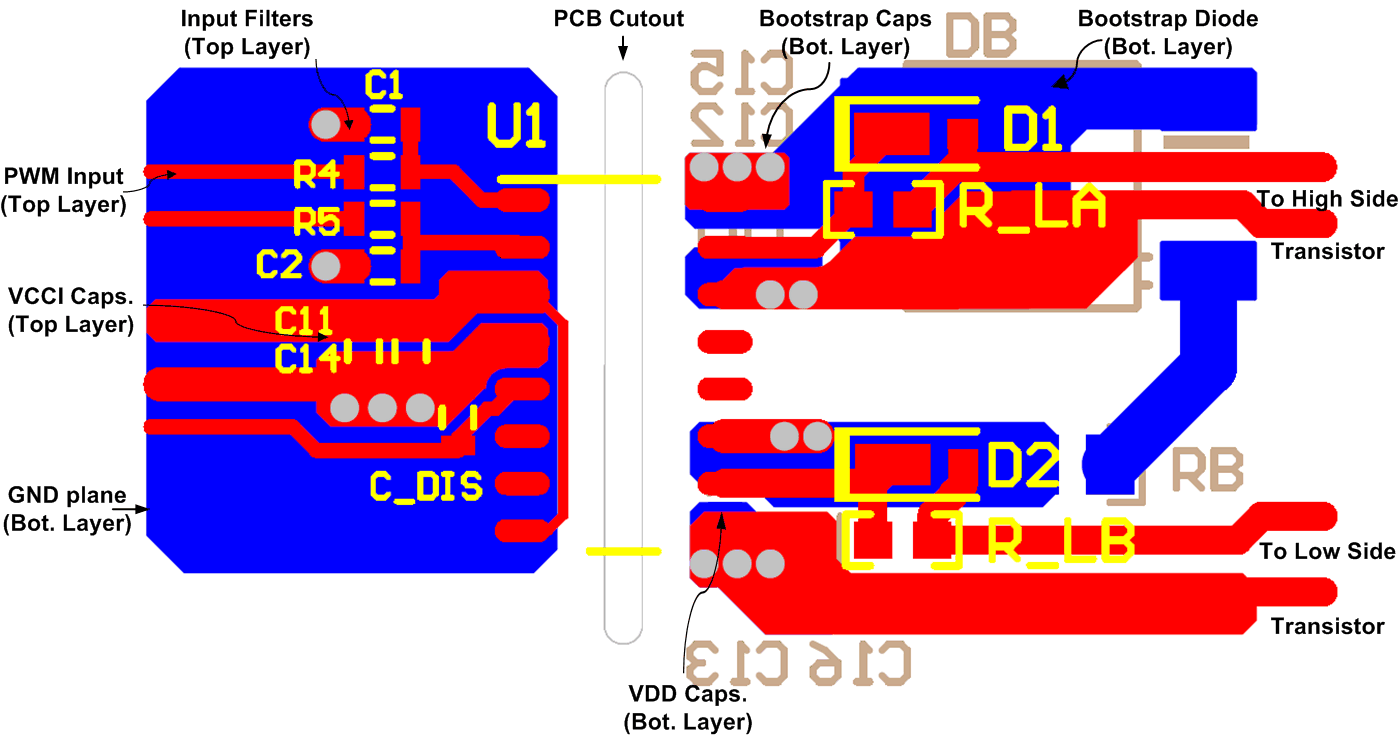
Figure 11-1 shows a 2-layer PCB layout example with the signals and key components labeled.
UCC21220 UCC21220A Layout ExampleFigure 11-1 Layout Example

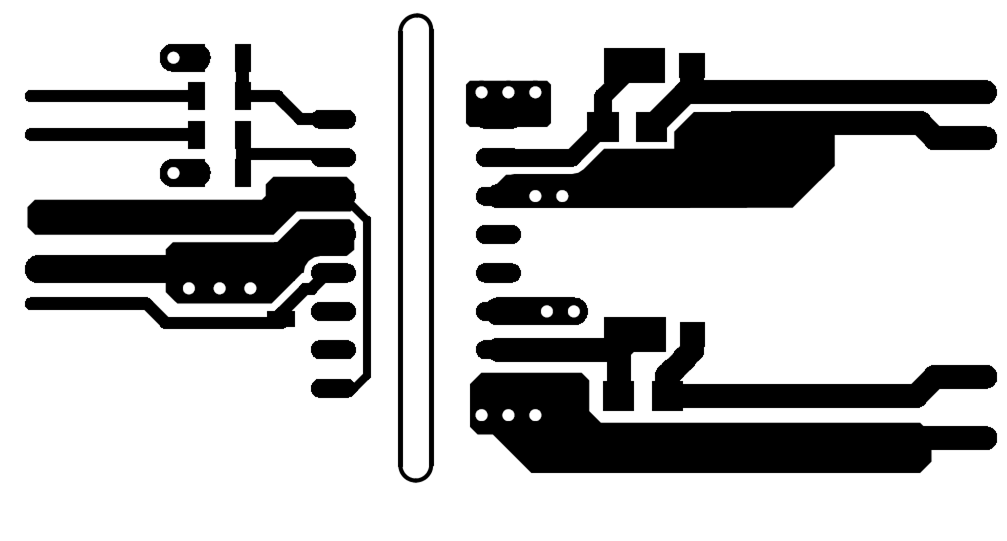
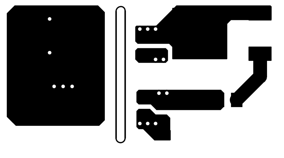
Figure 11-2 and Figure 11-3 shows top and bottom layer traces and copper.

Note:

There are no PCB traces or copper between the primary and secondary side, which ensures isolation performance.

PCB traces between the high-side and low-side gate drivers in the output stage are increased to maximize the creepage distance for high-voltage operation, which will also minimize cross-talk between the switching node VSSA (SW), where high dv/dt may exist, and the low-side gate drive due to the parasitic capacitance coupling.
UCC21220 UCC21220A Top Layer Traces and Copper
Figure 11-2 Top Layer Traces and Copper
UCC21220 UCC21220A Bottom Layer Traces and Copper
Figure 11-3 Bottom Layer Traces and Copper

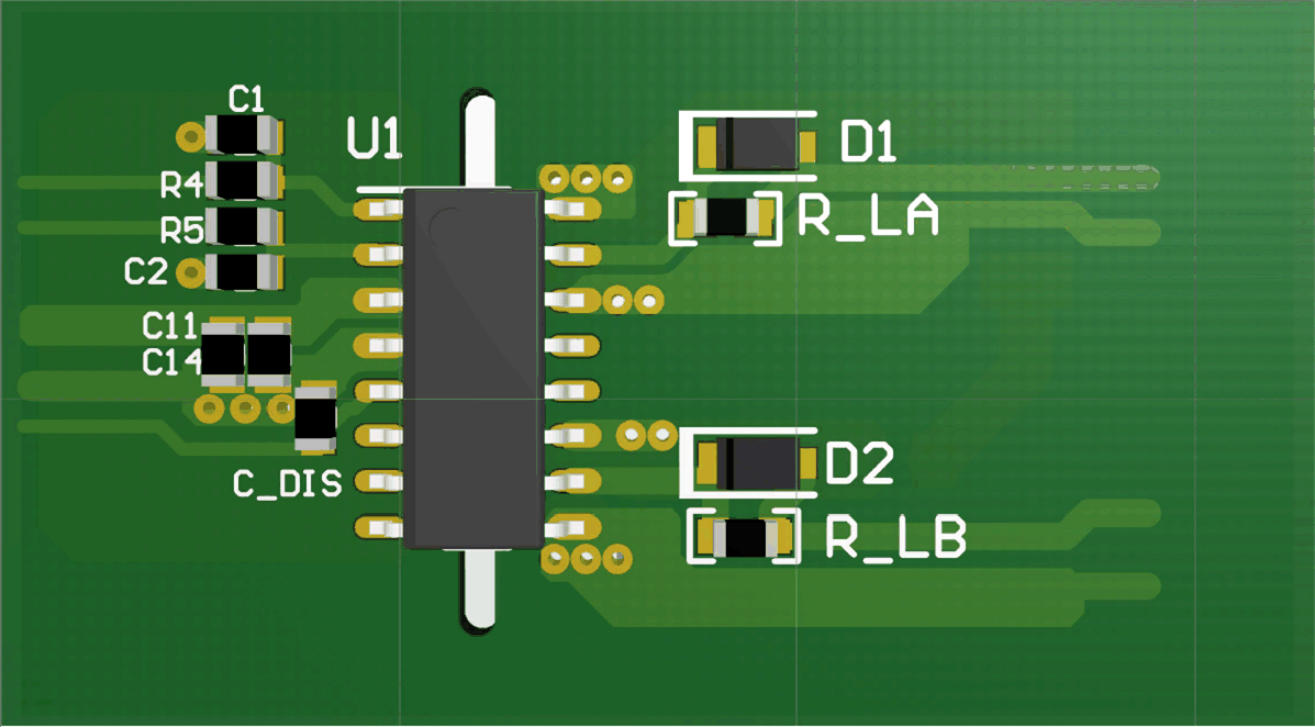
Figure 11-4 and Figure 11-5 are 3D layout pictures with top view and bottom views.

Note:

The location of the PCB cutout between the primary side and secondary sides, which ensures isolation performance.
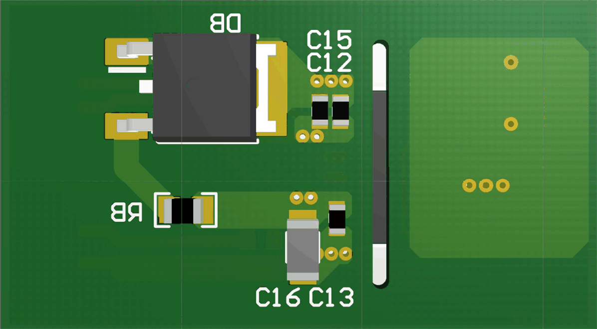
UCC21220 UCC21220A 3-D PCB Top View
Figure 11-4 3-D PCB Top View
UCC21220 UCC21220A 3-D PCB Bottom View
Figure 11-5 3-D PCB Bottom View