JAJSME3C March 2022 – June 2024 UCC21737-Q1
PRODUCTION DATA
- 1
- 1 特長
- 2 アプリケーション
- 3 概要
- 4 Pin Configuration and Functions
-
5 Specifications
- 5.1 Absolute Maximum Ratings
- 5.2 ESD Ratings
- 5.3 Recommended Operating Conditions
- 5.4 Thermal Information
- 5.5 Power Ratings
- 5.6 Insulation Specifications
- 5.7 Safety Limiting Values
- 5.8 Electrical Characteristics
- 5.9 Switching Characteristics
- 5.10 Insulation Characteristics Curves
- 5.11 Typical Characteristics
- 6 Parameter Measurement Information
-
7 Detailed Description
- 7.1 Overview
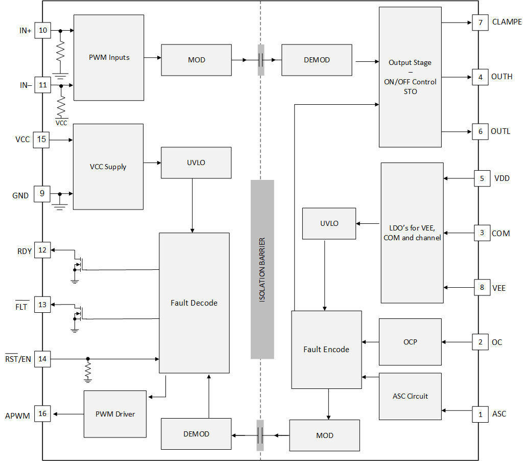
- 7.2 Functional Block Diagram
- 7.3
Feature Description
- 7.3.1 Power Supply
- 7.3.2 Driver Stage
- 7.3.3 VCC and VDD and VEE Undervoltage Lockout (UVLO)
- 7.3.4 Active Pulldown
- 7.3.5 Short Circuit Clamping
- 7.3.6 External Active Miller Clamp
- 7.3.7 Overcurrent and Short Circuit Protection
- 7.3.8 Soft Turn-off
- 7.3.9 Fault (FLT), Reset, and Enable (RST/EN)
- 7.3.10 ASC Support and APWM Monitor
- 7.4 Device Functional Modes
-
8 Applications and Implementation
- 8.1 Application Information
- 8.2
Typical Application
- 8.2.1 Design Requirements
- 8.2.2
Detailed Design Procedure
- 8.2.2.1 Input Filters for IN+, IN-, and RST/EN
- 8.2.2.2 PWM Interlock of IN+ and IN-
- 8.2.2.3 FLT, RDY, and RST/EN Pin Circuitry
- 8.2.2.4 RST/EN Pin Control
- 8.2.2.5 Turn-On and Turn-Off Gate Resistors
- 8.2.2.6 External Active Miller Clamp
- 8.2.2.7 Overcurrent and Short Circuit Protection
- 8.2.2.8 Higher Output Current Using an External Current Buffer
- 8.2.3 Application Curves
- 9 Power Supply Recommendations
- 10Layout
- 11Device and Documentation Support
- 12Revision History
- 13Mechanical, Packaging, and Orderable Information
パッケージ・オプション
メカニカル・データ(パッケージ|ピン)
- DW|16
サーマルパッド・メカニカル・データ
- DW|16
発注情報
7.2 Functional Block Diagram
