JAJSR77 September 2023 UCC21738-Q1
PRODUCTION DATA
- 1
- 1 特長
- 2 アプリケーション
- 3 概要
- 4 Revision History
- 5 Pin Configuration and Functions
-
6 Specifications
- 6.1 Absolute Maximum Ratings
- 6.2 ESD Ratings
- 6.3 Recommended Operating Conditions
- 6.4 Thermal Information
- 6.5 Power Ratings
- 6.6 Insulation Specifications
- 6.7 Safety Limiting Values
- 6.8 Electrical Characteristics
- 6.9 Switching Characteristics
- 6.10 Insulation Characteristics Curves
- 6.11 Typical Characteristics
- 7 Parameter Measurement Information
-
8 Detailed Description
- 8.1 Overview
- 8.2 Functional Block Diagram
- 8.3
Feature Description
- 8.3.1 Power Supply
- 8.3.2 Driver Stage
- 8.3.3 VCC and VDD Undervoltage Lockout (UVLO)
- 8.3.4 Active Pulldown
- 8.3.5 Short Circuit Clamping
- 8.3.6 External Active Miller Clamp
- 8.3.7 Overcurrent and Short Circuit Protection
- 8.3.8 Soft Turn-off
- 8.3.9 Fault (FLT), Reset, and Enable (RST/EN)
- 8.3.10 ASC Support and APWM Monitor
- 8.4 Device Functional Modes
-
9 Applications and Implementation
- 9.1 Application Information
- 9.2
Typical Application
- 9.2.1 Design Requirements
- 9.2.2
Detailed Design Procedure
- 9.2.2.1 Input Filters for IN+, IN-, and RST/EN
- 9.2.2.2 PWM Interlock of IN+ and IN-
- 9.2.2.3 FLT, RDY, and RST/EN Pin Circuitry
- 9.2.2.4 RST/EN Pin Control
- 9.2.2.5 Turn-On and Turn-Off Gate Resistors
- 9.2.2.6 External Active Miller Clamp
- 9.2.2.7 Overcurrent and Short Circuit Protection
- 9.2.2.8 Higher Output Current Using an External Current Buffer
- 9.2.3 Application Curves
- 10Power Supply Recommendations
- 11Layout
- 12Device and Documentation Support
- 13Mechanical, Packaging, and Orderable Information
8.3.2 Driver Stage
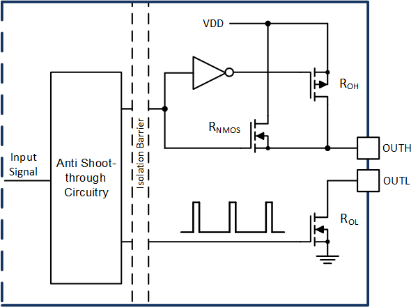
UCC21738-Q1 has ±10-A peak drive strength and is suitable for high power applications. The high drive strength can drive a SiC MOSFET module, IGBT module or paralleled discrete devices directly without an extra buffer stage. The UCC21738-Q1 can also be used to drive higher power modules or parallel modules with an extra buffer stage. Regardless of the values of VDD, the peak sink and source current can be kept at 10 A. The driver features an important safety function wherein, when the input pins are floating, the OUTH/OUTL is held low. The split output of the driver stage is depicted in Figure 8-1. The driver has rail-to-rail output by implementing a hybrid pullup structure with a P-Channel MOSFET in parallel with an N-Channel MOSFET, and an N-Channel MOSFET to pulldown. The pullup NMOS is the same as the pulldown NMOS, so the on resistance RNMOS is the same as ROL. The hybrid pullup structure delivers the highest peak-source current when it is most needed, during the Miller plateau region of the power semiconductor turn-on transient. The ROH in Figure 8-1 represents the on-resistance of the pullup P-Channel MOSFET. However, the effective pullup resistance is much smaller than ROH. Since the pullup N-Channel MOSFET has much smaller on-resistance than the P-Channel MOSFET, the pullup N-Channel MOSFET dominates most of the turn-on transient, until the voltage on OUTH pin is about 3V below VDD voltage. The effective resistance of the hybrid pullup structure during this period is about 2 x ROL . Then the P-Channel MOSFET pulls up the OUTH voltage to VDD rail. The low pullup impedance results in strong drive strength during the turn-on transient, which shortens the charging time of the input capacitance of the power semiconductor and reduces the turn-on switching loss.
The pulldown structure of the driver stage is implemented solely by a pulldown N-Channel MOSFET. This MOSFET can ensure the OUTL voltage be pulled down to VEE rail. The low pulldown impedance not only results in high sink current to reduce the turn-off time, but also helps to increase the noise immunity considering the Miller effect.
 Figure 8-1 Gate Driver
Output Stage