JAJSU20A December 2023 – April 2024 UCC23525
ADVANCE INFORMATION
- 1
- 1 特長
- 2 アプリケーション
- 3 概要
- 4 Pin Configuration and Function
- 5 Specifications
- 6 Parameter Measurement Information
- 7 Detailed Description
- 8 Application and Implementation
- 9 Power Supply Recommendations
- 10Layout
- 11Device and Documentation Support
- 12Revision History
- 13Mechanical, Packaging, and Orderable Information
デバイスごとのパッケージ図は、PDF版データシートをご参照ください。
メカニカル・データ(パッケージ|ピン)
- DWY|6
サーマルパッド・メカニカル・データ
8.2.2.4 Estimating Junction Temperature
Use Equation 15 to estimate the junction temperature (TJ) of UCC23525.
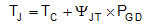
where
- TC is the UCC23525 case-top temperature measured with a thermocouple or some other instrument.
- ΨJT is the junction-to-top characterization parameter from the table.
Using the junction-to-top characterization parameter (ΨJT) instead of the junction-to-case thermal resistance (RθJC) can greatly improve the accuracy of the junction temperature estimation. The majority of the thermal energy of most ICs is released into the PCB through the package leads, whereas only a small percentage of the total energy is released through the top of the case (where thermocouple measurements are usually conducted). The RθJC resistance can only be used effectively when most of the thermal energy is released through the case, such as with metal packages or when a heat sink is applied to an IC package. In all other cases, use of RθJC will inaccurately estimate the true junction temperature. The ΨJT parameter is experimentally derived by assuming that the dominant energy leaving through the top of the IC will be similar in both the testing environment and the application environment. As long as the recommended layout guidelines are observed, junction temperature estimations can be made accurately to within a few degrees Celsius.