JAJSU20A December 2023 – April 2024 UCC23525
ADVANCE INFORMATION
- 1
- 1 特長
- 2 アプリケーション
- 3 概要
- 4 Pin Configuration and Function
- 5 Specifications
- 6 Parameter Measurement Information
- 7 Detailed Description
- 8 Application and Implementation
- 9 Power Supply Recommendations
- 10Layout
- 11Device and Documentation Support
- 12Revision History
- 13Mechanical, Packaging, and Orderable Information
デバイスごとのパッケージ図は、PDF版データシートをご参照ください。
メカニカル・データ(パッケージ|ピン)
- DWY|6
サーマルパッド・メカニカル・データ
10.2 Layout Example
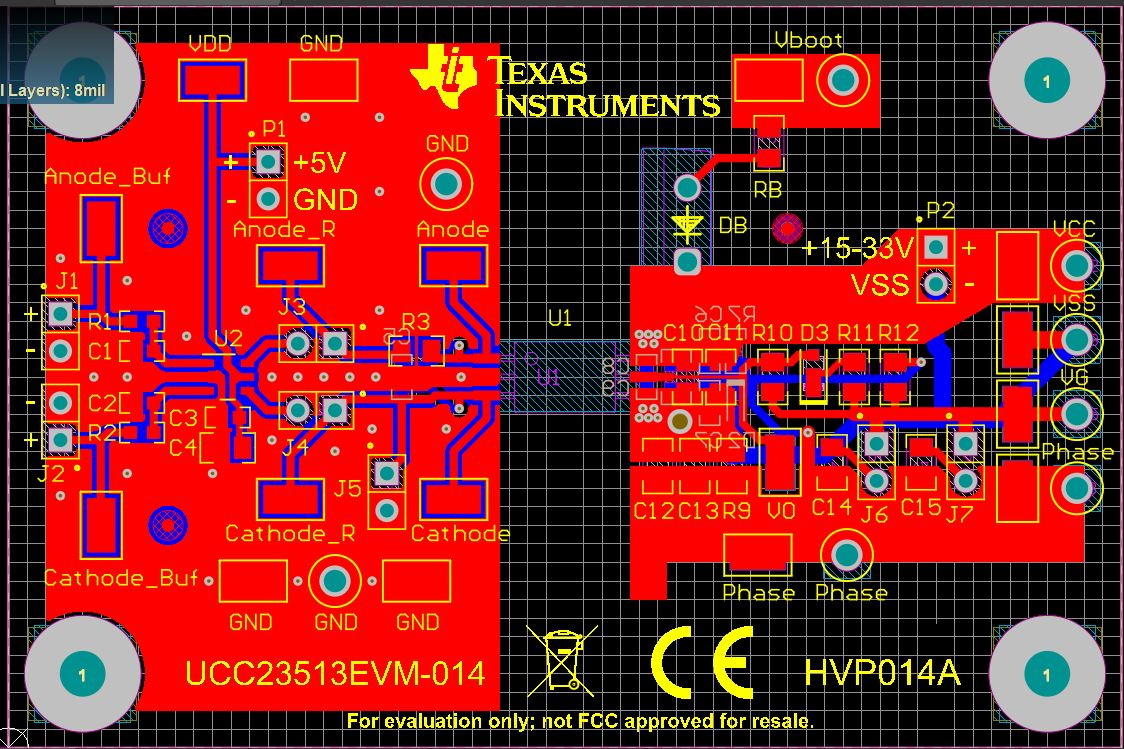
Figure 10-1 shows a PCB layout example with the signals and key components labeled.

A. No PCB traces or copper are
located between the primary and secondary side, which ensures isolation
performance.
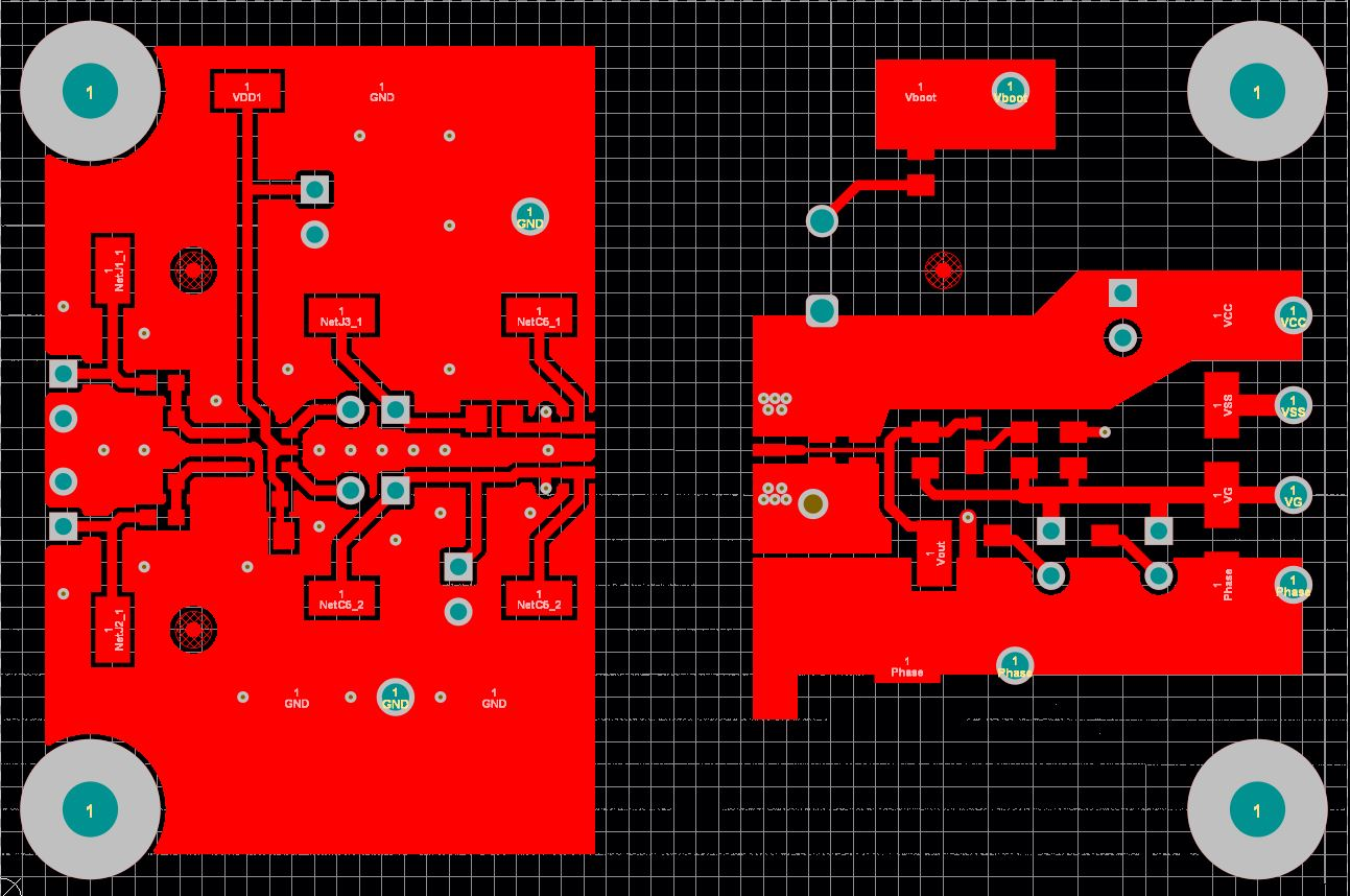
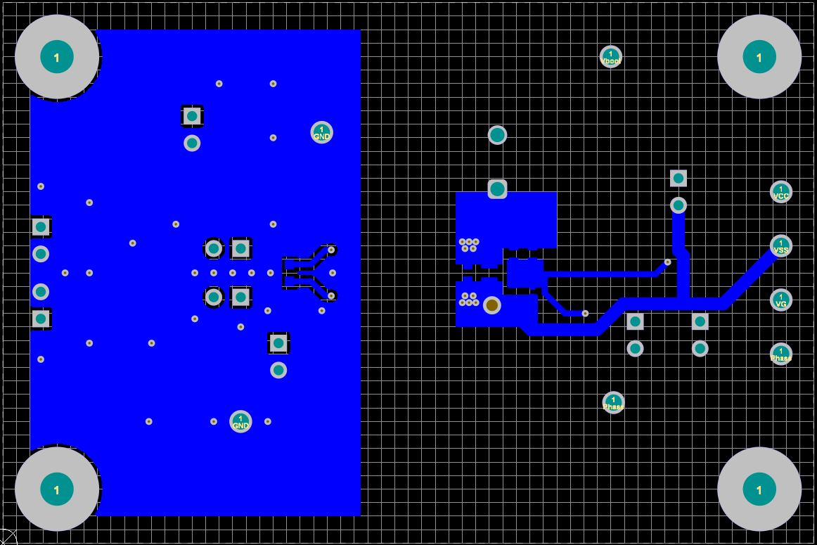
Figure 10-1 Layout ExampleFigure 10-2 and Figure 10-3 show the top and bottom layer traces and copper.
 Figure 10-2 Top-Layer Traces and
Copper
 Figure 10-3 Bottom-Layer Traces and Copper
(Flipped)
Figure 10-3 Bottom-Layer Traces and Copper
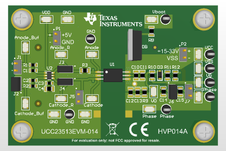
(Flipped)Figure 10-4 shows the 3D layout of the top view of the PCB.
 Figure 10-4 3-D PCB View