JAJSNN2B October 2023 – July 2024 UCC25660
PRODUCTION DATA
- 1
- 1 特長
- 2 アプリケーション
- 3 概要
- 4 Device Comparison Table
- 5 Pin Configuration and Functions
- 6 Specifications
-
7 Detailed Description
- 7.1 Overview
- 7.2 Functional Block Diagram
- 7.3 Feature Description
- 7.4 Protections
- 7.5 Device Functional Modes
-
8 Application and Implementation
- 8.1 Application Information
- 8.2
Typical Application
- 8.2.1 Design Requirements
- 8.2.2
Detailed Design Procedure
- 8.2.2.1 LLC Power Stage Requirements
- 8.2.2.2 LLC Gain Range
- 8.2.2.3 Select Ln and Qe
- 8.2.2.4 Determine Equivalent Load Resistance
- 8.2.2.5 Determine Component Parameters for LLC Resonant Circuit
- 8.2.2.6 LLC Primary-Side Currents
- 8.2.2.7 LLC Secondary-Side Currents
- 8.2.2.8 LLC Transformer
- 8.2.2.9 LLC Resonant Inductor
- 8.2.2.10 LLC Resonant Capacitor
- 8.2.2.11 LLC Primary-Side MOSFETs
- 8.2.2.12 Design Considerations for Adaptive Dead-Time
- 8.2.2.13 LLC Rectifier Diodes
- 8.2.2.14 LLC Output Capacitors
- 8.2.2.15 HV Pin Series Resistors
- 8.2.2.16 BLK Pin Voltage Divider
- 8.2.2.17 ISNS Pin Differentiator
- 8.2.2.18 TSET Pin
- 8.2.2.19 OVP/OTP Pin
- 8.2.2.20 Burst Mode Programming
- 8.2.2.21 Application Curves
- 8.3 Power Supply Recommendations
- 8.4 Layout
- 9 Revision History
- 10Mechanical, Packaging, and Orderable Information
8.2.2.18 TSET Pin
The TSET pin voltage is used to set the VCR integrator time constants and the minimum switching frequency. Depending on the selected option, OCP1 threshold, Timer gain (ks), Integrator component values (RVCR, RRAMP, CVCR), maximum dead time would be set.
For this design, TSET option #4 is selected. So, for option #4, TSET pin voltage needs to be between 0.742V to 0.850V as given in table TSET Programming Options table . A 1M ohm (RTSET_upper) and a 191kΩ (RTSET_lower) are used at the TSET pin. Then the TSET pin voltage will be
Then the Equation 4 will become
where previously chosen values of RISNS, CISNS, CR, RBLKupper, RBLKlower, Integrator time constants values of TSET option #4 are used to obtain this relation.
Here for calculating Pin, 92% efficiency is considered in the following expression.
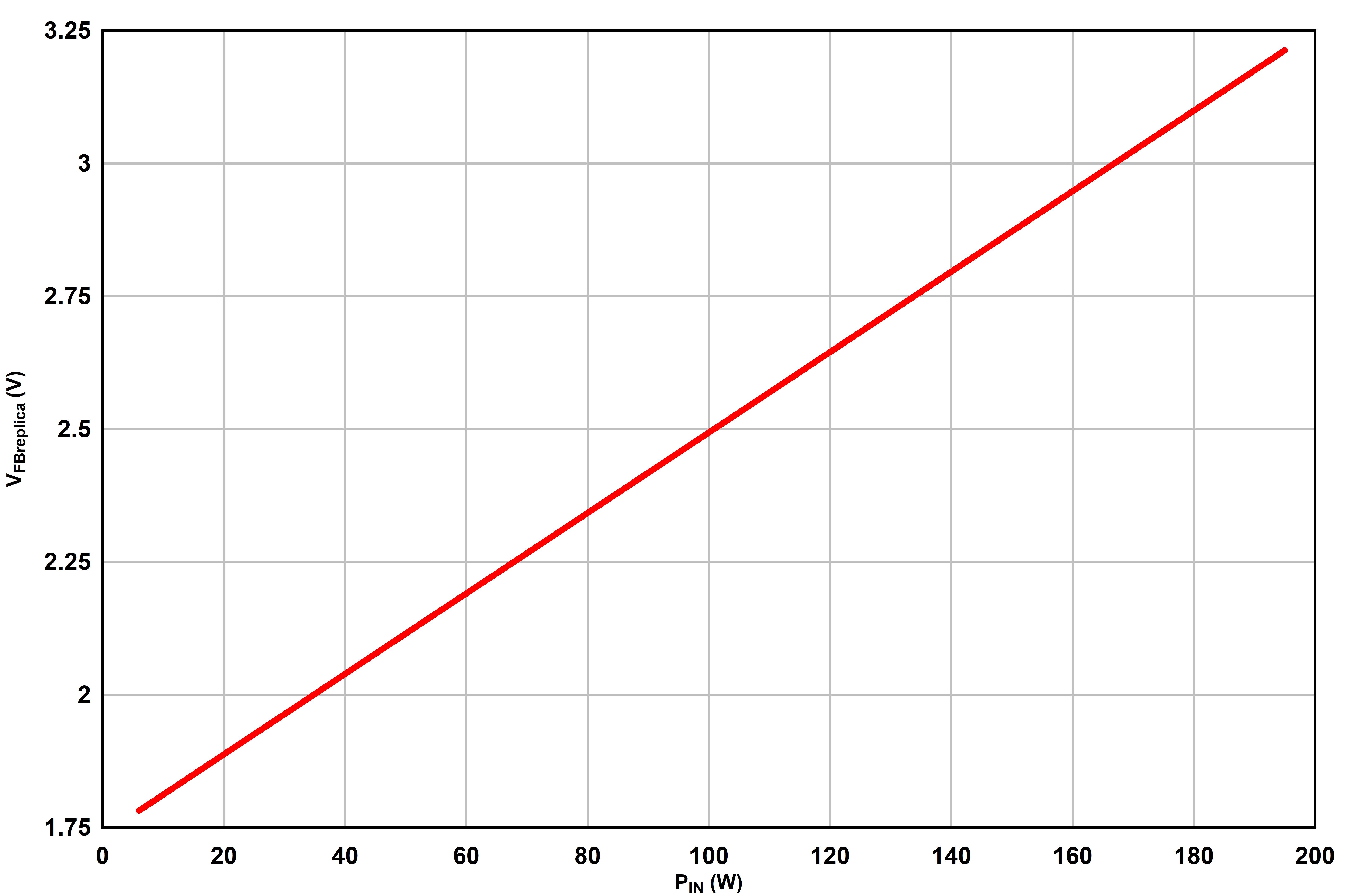
Figure 8-2 shows the FBReplica voltage with respect to the input power of the LLC.
 Figure 8-2 FBReplica vs
Pin
Figure 8-2 FBReplica vs
PinThe FBReplica voltage can be measured by inserting a 10-kΩ resistor between the feedback optocoupler emitter and ground. Assume the voltage measured on the 10-kΩ resistor is V10k. Then FBReplica voltage can be calculated as: