JAJSNN2B October 2023 – July 2024 UCC25660
PRODUCTION DATA
- 1
- 1 特長
- 2 アプリケーション
- 3 概要
- 4 Device Comparison Table
- 5 Pin Configuration and Functions
- 6 Specifications
-
7 Detailed Description
- 7.1 Overview
- 7.2 Functional Block Diagram
- 7.3 Feature Description
- 7.4 Protections
- 7.5 Device Functional Modes
-
8 Application and Implementation
- 8.1 Application Information
- 8.2
Typical Application
- 8.2.1 Design Requirements
- 8.2.2
Detailed Design Procedure
- 8.2.2.1 LLC Power Stage Requirements
- 8.2.2.2 LLC Gain Range
- 8.2.2.3 Select Ln and Qe
- 8.2.2.4 Determine Equivalent Load Resistance
- 8.2.2.5 Determine Component Parameters for LLC Resonant Circuit
- 8.2.2.6 LLC Primary-Side Currents
- 8.2.2.7 LLC Secondary-Side Currents
- 8.2.2.8 LLC Transformer
- 8.2.2.9 LLC Resonant Inductor
- 8.2.2.10 LLC Resonant Capacitor
- 8.2.2.11 LLC Primary-Side MOSFETs
- 8.2.2.12 Design Considerations for Adaptive Dead-Time
- 8.2.2.13 LLC Rectifier Diodes
- 8.2.2.14 LLC Output Capacitors
- 8.2.2.15 HV Pin Series Resistors
- 8.2.2.16 BLK Pin Voltage Divider
- 8.2.2.17 ISNS Pin Differentiator
- 8.2.2.18 TSET Pin
- 8.2.2.19 OVP/OTP Pin
- 8.2.2.20 Burst Mode Programming
- 8.2.2.21 Application Curves
- 8.3 Power Supply Recommendations
- 8.4 Layout
- 9 Revision History
- 10Mechanical, Packaging, and Orderable Information
7.3.5.1 Brown in and Brown out Tresholds and Options
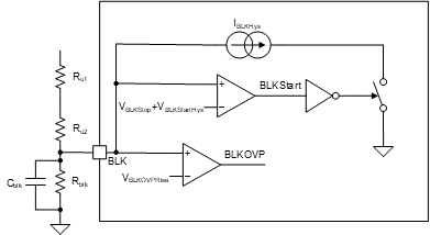
UCC25660x ファミリ provides programmable brown-in and brown-out threshold. When the voltage on the BLK pin falls below VBLKStop, the controller enters brown out state and stops switching. In the brown-out state, an additional current sink is turned on to draw IBLKHys form the BLK pin. By changing the equivalent resistance connected to the pin externally, the actual brown-in voltage can be programmed.
 Figure 7-6 BLK Pin Input Voltage Sensing
Architecture
Figure 7-6 BLK Pin Input Voltage Sensing
ArchitectureWhen brown-out is detected, the controller stops switching. If BLK voltage rises above the brown-in voltage, the controller immediately begins soft start and does not wait for fault idle time.
In the variants that have the BLK OVP option enabled, if the BLK pin voltage rises above the OVP threshold, the controller stops switching and move to the fault state. After the fault idle time, the controller checks if the OVP condition is cleared. If the OVP condition is removed, the controller begins recovery and soft start. If the OVP condition is not cleared, the controller stays off and waits until the OVP condition is cleared.