JAJSNN2B October 2023 – July 2024 UCC25660
PRODUCTION DATA
- 1
- 1 特長
- 2 アプリケーション
- 3 概要
- 4 Device Comparison Table
- 5 Pin Configuration and Functions
- 6 Specifications
-
7 Detailed Description
- 7.1 Overview
- 7.2 Functional Block Diagram
- 7.3 Feature Description
- 7.4 Protections
- 7.5 Device Functional Modes
-
8 Application and Implementation
- 8.1 Application Information
- 8.2
Typical Application
- 8.2.1 Design Requirements
- 8.2.2
Detailed Design Procedure
- 8.2.2.1 LLC Power Stage Requirements
- 8.2.2.2 LLC Gain Range
- 8.2.2.3 Select Ln and Qe
- 8.2.2.4 Determine Equivalent Load Resistance
- 8.2.2.5 Determine Component Parameters for LLC Resonant Circuit
- 8.2.2.6 LLC Primary-Side Currents
- 8.2.2.7 LLC Secondary-Side Currents
- 8.2.2.8 LLC Transformer
- 8.2.2.9 LLC Resonant Inductor
- 8.2.2.10 LLC Resonant Capacitor
- 8.2.2.11 LLC Primary-Side MOSFETs
- 8.2.2.12 Design Considerations for Adaptive Dead-Time
- 8.2.2.13 LLC Rectifier Diodes
- 8.2.2.14 LLC Output Capacitors
- 8.2.2.15 HV Pin Series Resistors
- 8.2.2.16 BLK Pin Voltage Divider
- 8.2.2.17 ISNS Pin Differentiator
- 8.2.2.18 TSET Pin
- 8.2.2.19 OVP/OTP Pin
- 8.2.2.20 Burst Mode Programming
- 8.2.2.21 Application Curves
- 8.3 Power Supply Recommendations
- 8.4 Layout
- 9 Revision History
- 10Mechanical, Packaging, and Orderable Information
8.2.2.12 Design Considerations for Adaptive Dead-Time
After the resonant tank is designed and the primary side MOSFET is selected, the ZVS operation of the converter needs to be double checked. ZVS can only be achieved when there is enough current left in the resonant inductor at the gate turn off edge to discharge the switch node. UC256604 implements adaptive dead-time based on the slewing of the switch node. The slew detection circuit has a detection range of 0.1V/ns to 200V/ns.
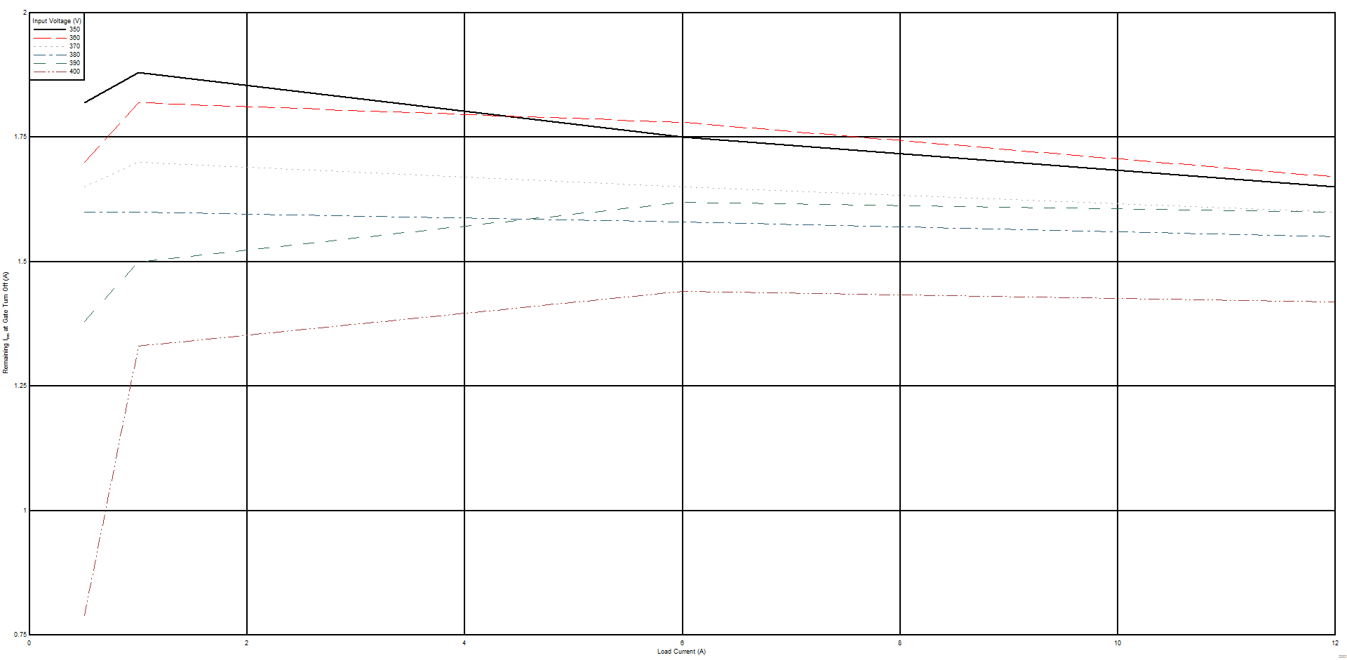
To check the ZVS operation, a series of time domain simulations are conducted, and the resonant current at the gate turn off edges are captured. An example plot is shown below:
 Figure 8-1 Adaptive Dead-Time
The figure above assumes the maximum switching frequency occurs at 5% load, and system starts to burst at 5% load.
From this plot, the minimum resonant current left in the tank is Imin = 0.8A in the interested operation range. In order to calculate the slew rate, the primary side switch node parasitic capacitance must be known. This value can be estimated from the MOSFET datasheet. In this case, Cswitchnode = 400pF. The minimum slew rate is given by:

This is larger than 0.1V/ns minimum detectable slew rate.