JAJSNN2B October 2023 – July 2024 UCC25660
PRODUCTION DATA
- 1
- 1 特長
- 2 アプリケーション
- 3 概要
- 4 Device Comparison Table
- 5 Pin Configuration and Functions
- 6 Specifications
-
7 Detailed Description
- 7.1 Overview
- 7.2 Functional Block Diagram
- 7.3 Feature Description
- 7.4 Protections
- 7.5 Device Functional Modes
-
8 Application and Implementation
- 8.1 Application Information
- 8.2
Typical Application
- 8.2.1 Design Requirements
- 8.2.2
Detailed Design Procedure
- 8.2.2.1 LLC Power Stage Requirements
- 8.2.2.2 LLC Gain Range
- 8.2.2.3 Select Ln and Qe
- 8.2.2.4 Determine Equivalent Load Resistance
- 8.2.2.5 Determine Component Parameters for LLC Resonant Circuit
- 8.2.2.6 LLC Primary-Side Currents
- 8.2.2.7 LLC Secondary-Side Currents
- 8.2.2.8 LLC Transformer
- 8.2.2.9 LLC Resonant Inductor
- 8.2.2.10 LLC Resonant Capacitor
- 8.2.2.11 LLC Primary-Side MOSFETs
- 8.2.2.12 Design Considerations for Adaptive Dead-Time
- 8.2.2.13 LLC Rectifier Diodes
- 8.2.2.14 LLC Output Capacitors
- 8.2.2.15 HV Pin Series Resistors
- 8.2.2.16 BLK Pin Voltage Divider
- 8.2.2.17 ISNS Pin Differentiator
- 8.2.2.18 TSET Pin
- 8.2.2.19 OVP/OTP Pin
- 8.2.2.20 Burst Mode Programming
- 8.2.2.21 Application Curves
- 8.3 Power Supply Recommendations
- 8.4 Layout
- 9 Revision History
- 10Mechanical, Packaging, and Orderable Information
7.1 Overview
The UCC25660x ファミリ is a fully featured LLC resonant controller for isolated power supplies. It incorporates high level of integration and several design features to accommodate wide input/output voltage operation, high power density and increased reliability of the LLC power stage.
The device's novel control scheme Input Power Proportional Control (IPPC) offers excellent transient performance inherent in the current mode controls, while enabling a linear relationship between input power and control signal across wide input and output voltage variation. The IPPC control enables consistent light load, burst mode performance operation across a wide input/output voltage variation.
Some of the new features in UCC25660x ファミリ are specified below:
- IPPC Control enables better burst mode and dynamic response under wide input/output voltage operation.
- New operation modes to increase light
load efficiency while reducing audible noise.
- High-frequency (HF) pulse skip for improved light load efficiency.
- Low-frequency (LF) burst mode for reduced stand by power consumption.
- Programable light load / burst mode thresholds.
- Adaptive burst mode threshold adjustment to accommodate input voltage change.
- Up to 750kHz full-load switching frequency enables high power density designs.
- Combined resonant current sensing with internal control voltage generation, improves control robustness.
- Input feed forward.
- Integrated protections include:
- Fast 50ns cycle-by-cycle current limiting.
- OCP fault to protect under short circuit conditions.
- Over Power Protection (OPP) to limit peak input power.
- ZCS (Zero Current Switching) avoidance scheme to eliminate capacitive region operation.
- Adaptive soft start for reduced inrush current and eliminating reverse recovery at startup.
- External OVP/OTP protection.
- Input & bias supply (VCCP) UVLO.
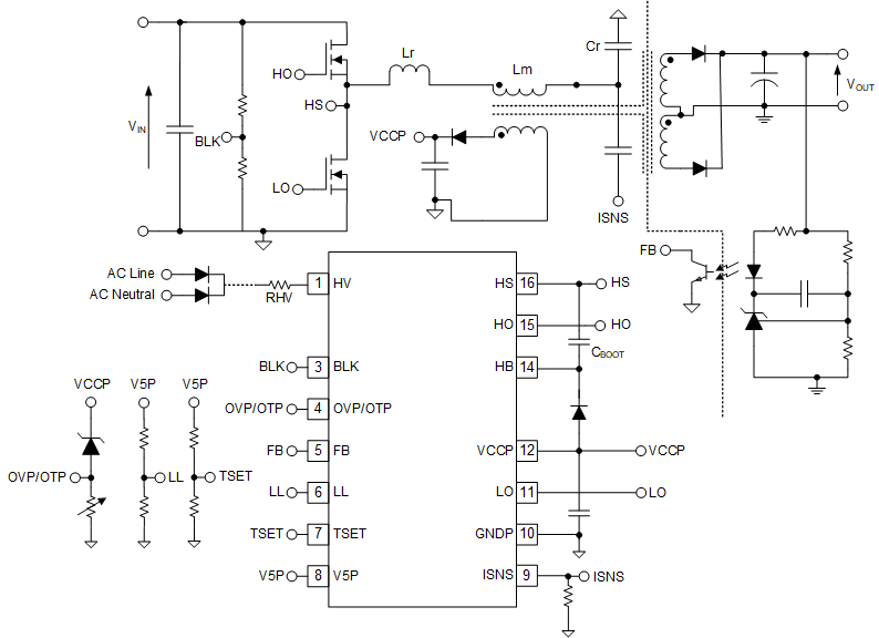
 Figure 7-1 Simplified Application
Schematic