SLUSAT7G November 2011 – July 2024 UCC27211
PRODUCTION DATA
- 1
- 1 Features
- 2 Applications
- 3 Description
- 4 Pin Configuration and Functions
- 5 Specifications
- 6 Detailed Description
- 7 Application and Implementation
- 8 Power Supply Recommendations
- 9 Layout
- 10Device and Documentation Support
- 11Revision History
- 12Mechanical, Packaging, and Orderable Information
パッケージ・オプション
デバイスごとのパッケージ図は、PDF版データシートをご参照ください。
メカニカル・データ(パッケージ|ピン)
- D|8
- DRM|8
- DPR|10
- DDA|8
サーマルパッド・メカニカル・データ
発注情報
4 Pin Configuration and Functions
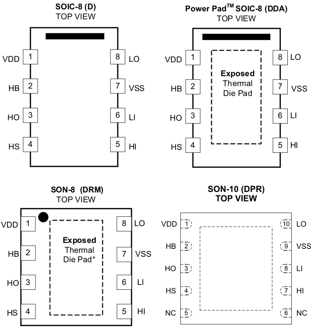
Table 4-1 Pin Functions
| PIN | I/O | DESCRIPTION | ||
|---|---|---|---|---|
| NAME | D/DDA/DRM | DPR | ||
| VDD | 1 | 1 | P | Positive supply to the lower-gate driver. Decouple this pin to VSS (GND). Typical decoupling capacitor range is 0.22µF to 4.7µF (See (2)). |
| HB | 2 | 2 | P | High-side bootstrap supply. The bootstrap diode is on-chip but the external bootstrap capacitor is required. Connect positive side of the bootstrap capacitor to this pin. Typical range of HB bypass capacitor is 0.022µF to 0.1µF. The capacitor value is dependant on the gate charge of the high-side MOSFET and should also be selected based on speed and ripple criteria |
| HO | 3 | 3 | O | High-side output. Connect to the gate of the high-side power MOSFET. |
| HS | 4 | 4 | P | High-side source connection. Connect to source of high-side power MOSFET. Connect the negative side of bootstrap capacitor to this pin. |
| HI | 5 | 7 | I | High-side input.(3) |
| LI | 6 | 8 | I | Low-side input.(3) |
| VSS | 7 | 9 | G | Negative supply terminal for the device which is generally grounded. |
| LO | 8 | 10 | O | Low-side output. Connect to the gate of the low-side power MOSFET. |
| N/C | — | 5/6 | — | Not connected. |
| PowerPAD™(1) | Pad | Pad | G | Used on the DDA, DRM and DPR packages only. Electrically referenced to VSS (GND). Connect to a large thermal mass trace or GND plane to dramatically improve thermal performance. |
(1) The PowerPAD™ is not directly connected to any leads of the
package. However it is electrically and thermally connected to the substrate
which is the ground of the device.
(2) For cold temperature applications we recommend the upper
capacitance range. Attention should also be made to PCB layout - see Section 9.
(3) HI or LI input is assumed to connect to a low impedance source
signal. The source output impedance is assumed less than 100Ω. If the source
impedance is greater than 100Ω, add a bypassing capacitor, each, between HI and
VSS and between LI and VSS. The added capacitor value depends on the noise
levels presented on the pins, typically from 1 nF to 10nF should be effective to
eliminate the possible noise effect. When noise is present on two pins, HI or
LI, the effect is to cause HO and LO malfunctions to have wrong logic
outputs.