JAJSEZ0B August   2014  – January 2024 UCC27511A-Q1

PRODUCTION DATA  

  1.   1
  2. 特長
  3. アプリケーション
  4. 概要
  5. Pin Configuration and Functions
  6. Specifications
    1. 5.1 Absolute Maximum Ratings
    2. 5.2 Handling Ratings
    3. 5.3 Recommended Operating Conditions
    4. 5.4 Thermal Information
    5. 5.5 Electrical Characteristics
    6. 5.6 Switching Characteristics
    7. 5.7 Typical Characteristics
  7. Detailed Description
    1. 6.1 Overview
    2. 6.2 Functional Block Diagram
    3. 6.3 Feature Description
      1. 6.3.1 VDD and Undervoltage Lockout
      2. 6.3.2 Operating Supply Current
      3. 6.3.3 Input Stage
      4. 6.3.4 Enable Function
      5. 6.3.5 Output Stage
      6. 6.3.6 Low Propagation Delays
    4. 6.4 Device Functional Modes
  8. Application and Implementation
    1. 7.1 Application Information
    2. 7.2 Typical Application
      1. 7.2.1 Design Requirements
      2. 7.2.2 Detailed Design Procedure
        1. 7.2.2.1 Input-to-Output Logic
        2. 7.2.2.2 Input Threshold Type
        3. 7.2.2.3 VDD Bias Supply Voltage
        4. 7.2.2.4 Peak Source and Sink Currents
        5. 7.2.2.5 Enable and Disable Function
        6. 7.2.2.6 Propagation Delay
        7. 7.2.2.7 Thermal Information
        8. 7.2.2.8 Power Dissipation
      3. 7.2.3 Application Curves
  9. Power Supply Recommendations
  10. Layout
    1. 9.1 Layout Guidelines
    2. 9.2 Layout Example
  11. 10Device and Documentation Support
    1. 10.1 Device Support
      1. 10.1.1 サード・パーティ製品に関する免責事項
    2. 10.2 ドキュメントの更新通知を受け取る方法
    3. 10.3 サポート・リソース
    4. 10.4 Trademarks
    5. 10.5 静電気放電に関する注意事項
    6. 10.6 用語集
  12. 11Revision History
  13. 12Mechanical, Packaging, and Orderable Information

パッケージ・オプション

メカニカル・データ(パッケージ|ピン)
サーマルパッド・メカニカル・データ
発注情報

Typical Application

Figure 7-1 shows the typical application of UCC27511A-Q1 device when used as a gate driver for the power MOSFET in a boost-converter application (for example, AC-DC power factor correction in AC-DC chargers for electric vehicles). In this application the UCC27511A-Q1 device is used in the non-inverting input configuration.
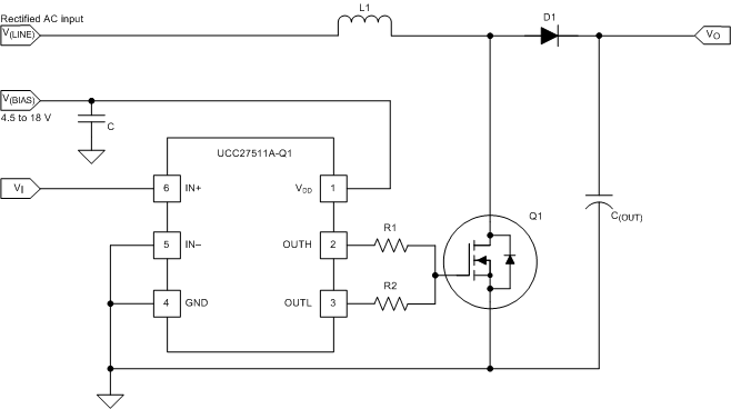
GUID-236FDE52-D9FB-4256-9C90-D68A2E08D879-low.gif Figure 7-1 Typical Application in PFC Power Stage