SLUSAW9F February 2012 – November 2014 UCC27511 , UCC27512
PRODUCTION DATA.
- 1 Features
- 2 Applications
- 3 Description
- 4 Revision History
- 5 Description (Continued)
- 6 UCC2751x Product Family
- 7 Pin Configuration and Functions
- 8 Specifications
- 9 Detailed Description
- 10Application and Implementation
- 11Power Supply Recommendations
- 12Layout
- 13Device and Documentation Support
- 14Mechanical, Packaging, and Orderable Information
パッケージ・オプション
メカニカル・データ(パッケージ|ピン)
- DRS|6
サーマルパッド・メカニカル・データ
- DRS|6
発注情報
1 Features
- Low-Cost Gate-Driver Device Offering Superior Replacement of NPN and PNP Discrete Solutions
- 4-A Peak Source and 8-A Peak Sink Asymmetrical Drive
- Strong Sink Current Offers Enhanced Immunity Against Miller Turnon
- Split Output Configuration (Allows Easy and Independent Adjustment of Turnon and Turnoff Speeds) in the UCC27511 Saves 1 Diode
- Fast Propagation Delays (13-ns Typical)
- Fast Rise and Fall Times (9-ns and 7-ns Typical)
- 4.5-V to 18-V Single Supply Range
- Outputs Held Low During VDD UVLO (Ensures Glitch-Free Operation at Power Up and Power Down)
- TTL and CMOS Compatible Input-Logic Threshold (Independent of Supply Voltage)
- Hysteretic-Logic Thresholds for High-Noise Immunity
- Dual-Input Design (Choice of an Inverting (IN– Pin) or Noninverting (IN+ Pin) Driver Configuration)
- Unused Input Pin can be Used for Enable or Disable Function
- Output Held Low When Input Pins Are Floating
- Input Pin Absolute Maximum Voltage Levels Not Restricted by VDD Pin Bias Supply Voltage
- Operating Temperature Range of –40°C to 140°C
- 6-Pin DBV (SOT-23) and 6-Pin DRS (3-mm ×
3-mm WSON With Exposed Thermal Pad) Package Options
2 Applications
- Switched-Mode Power Supplies
- DC-to-DC Converters
- Companion Gate-Driver Devices for Digital Power Controllers
- Solar Power, Motor Control, UPS
- Gate Driver for Emerging Wide Band-Gap Power Devices (such as GaN)
3 Description
The UCC27511 and UCC27512 single-channel, high-speed, low-side gate-driver device can effectively drive MOSFET and IGBT power switches. Using a design that inherently minimizes shoot-through current, UCC27511 and UCC27512 are capable of sourcing and sinking high peak-current pulses into capacitive loads offering rail-to-rail drive capability and extremely small propagation delay, typically 13 ns.
Device Information(1)
| PART NUMBER | PACKAGE | BODY SIZE (NOM) |
|---|---|---|
| UCC27511 | SOT-23 (6) | 2.90 mm x 1.60 mm |
| UCC27512 | WSON (6) | 3.00 mm x 3.00 mm |
- For all available packages, see the orderable addendum at the end of the datasheet.
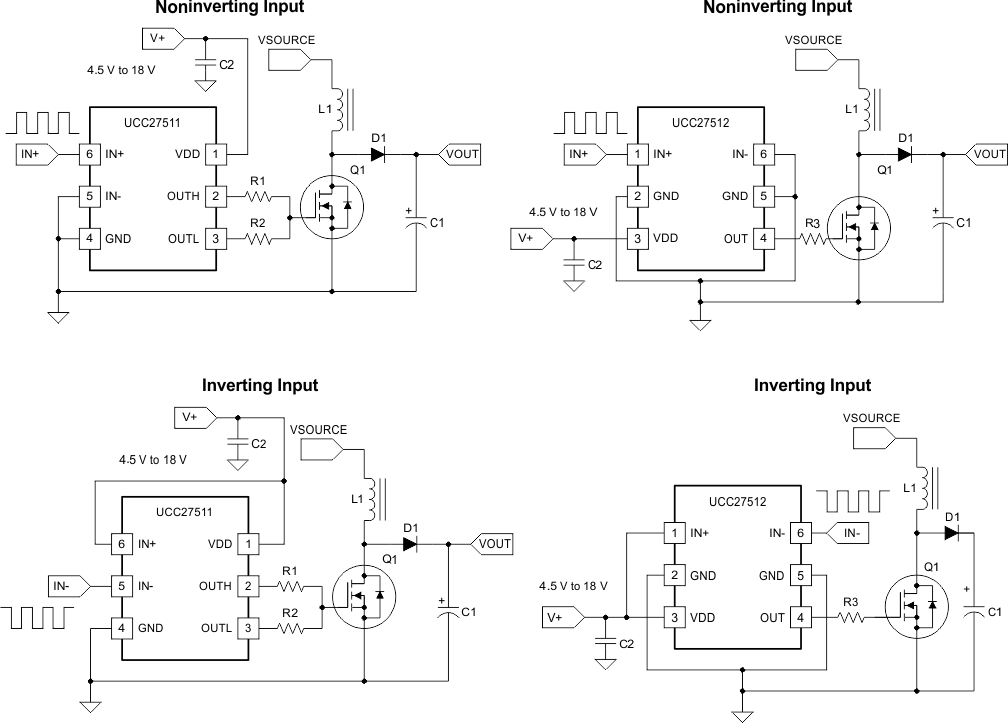
Typical Application Diagrams