JAJSD39 April   2017 UCC27524A1-Q1

PRODUCTION DATA.  

  1. 特長
  2. アプリケーション
  3. 概要
  4. 改訂履歴
  5. 概要(続き)
  6. Pin Configuration and Functions
  7. Specifications
    1. 7.1 Absolute Maximum Ratings
    2. 7.2 ESD Ratings
    3. 7.3 Recommended Operating Conditions
    4. 7.4 Thermal Information
    5. 7.5 Electrical Characteristics
    6. 7.6 Switching Characteristics
    7. 7.7 Typical Characteristics
  8. Detailed Description
    1. 8.1 Overview
    2. 8.2 Functional Block Diagram
    3. 8.3 Feature Description
      1. 8.3.1 Operating Supply Current
      2. 8.3.2 Input Stage
      3. 8.3.3 Enable Function
      4. 8.3.4 Output Stage
      5. 8.3.5 Low Propagation Delays And Tightly Matched Outputs
    4. 8.4 Device Functional Modes
  9. Application and Implementation
    1. 9.1 Application Information
    2. 9.2 Typical Application
      1. 9.2.1 Design Requirements
      2. 9.2.2 Detailed Design Procedure
        1. 9.2.2.1 VDD and Undervoltage Lockout
        2. 9.2.2.2 Drive Current and Power Dissipation
      3. 9.2.3 Application Curves
  10. 10Power Supply Recommendations
  11. 11Layout
    1. 11.1 Layout Guidelines
    2. 11.2 Layout Example
    3. 11.3 Thermal Considerations
  12. 12デバイスおよびドキュメントのサポート
    1. 12.1 コミュニティ・リソース
    2. 12.2 商標
    3. 12.3 静電気放電に関する注意事項
    4. 12.4 Glossary
  13. 13メカニカル、パッケージ、および注文情報

パッケージ・オプション

メカニカル・データ(パッケージ|ピン)
サーマルパッド・メカニカル・データ
発注情報

Pin Configuration and Functions

DGN Package
8-Pin MSOP-PowerPAD
Top View
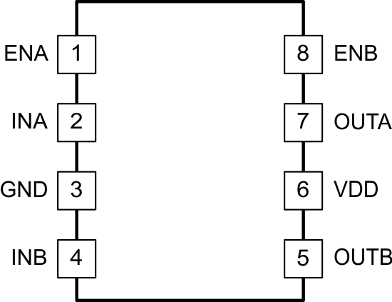
UCC27524A1-Q1 pin_lusbp4.gif

Pin Functions

PIN I/O DESCRIPTION
NAME NO.
ENA 1 I Enable input for Channel A: ENA is biased LOW to disable the Channel A output regardless of the INA state. ENA is biased HIGH or left floating to enable the Channel A output. ENA is allowed to float; hence the pin-to-pin compatibility with the UCC2732X N/C pin.
ENB 8 I Enable input for Channel B: ENB is biased LOW to disables the Channel B output regardless of the INB state. ENB is biased HIGH or left floating to enable Channel B output. ENB is allowed to float hence; the pin-to-pin compatibility with the UCC2752A N/C pin.
GND 3 - Ground: All signals are referenced to this pin.
INA 2 I Input to Channel A: INA is the non-inverting input in the UCC27524A1-Q1 device. OUTA is held LOW if INA is unbiased or floating.
INB 4 I Input to Channel B: INB is the non-inverting input in the UCC27524A1-Q1 device. OUTB is held LOW if INB is unbiased or floating.
OUTA 7 O Output of Channel A
OUTB 5 O Output of Channel B
VDD 6 I Bias supply input