JAJSD39 April 2017 UCC27524A1-Q1
PRODUCTION DATA.
7 Specifications
7.1 Absolute Maximum Ratings
over operating free-air temperature range (unless otherwise noted)(1)| MIN | MAX | UNIT | ||
|---|---|---|---|---|
| Supply voltage | VDD | –0.3 | 20 | V |
| OUTA, OUTB voltage | DC | –0.3 | VDD + 0.3 | V |
| Repetitive pulse < 200 ns(3) | –2 | VDD + 0.3 | V | |
| Output continuous source/sink current | IOUT_DC | 0.3 | A | |
| Output pulsed source/sink current (0.5 µs) | IOUT_pulsed | 5 | A | |
| INA, INB, ENA, ENB voltage(2) | –5 | 20 | V | |
| Operating virtual junction temperature, TJ | –40 | 150 | °C | |
| Storage temperature, Tstg | –65 | 150 | °C | |
(1) Stresses beyond those listed under Absolute Maximum Ratings may cause permanent damage to the device. These are stress ratings only, which do not imply functional operation of the device at these or any other conditions beyond those indicated under Recommended Operating Conditions. Exposure to absolute-maximum-rated conditions for extended periods may affect device reliability.
(2) The maximum voltage on the Input and Enable pins is not restricted by the voltage on the VDD pin.
(3) Values are verified by characterization on bench.
7.2 ESD Ratings
| VALUE | UNIT | |||
|---|---|---|---|---|
| V(ESD) | Electrostatic discharge | Human-body model (HBM), per AEC Q100-002(1) | ±2000 | V |
| Charged-device model (CDM), per AEC Q100-011 | ±750 | |||
(1) AEC Q100-002 indicates that HBM stressing shall be in accordance with the ANSI/ESDA/JEDEC JS-001 specification.
7.3 Recommended Operating Conditions
over operating free-air temperature range (unless otherwise noted)| MIN | NOM | MAX | UNIT | |
|---|---|---|---|---|
| Supply voltage, VDD | 4.5 | 12 | 18 | V |
| Operating junction temperature | –40 | 140 | °C | |
| Input voltage, INA, INB | –2 | 18 | V | |
| Enable voltage, ENA and ENB | –2 | 18 | V |
7.4 Thermal Information
| THERMAL METRIC(1) | UCC27524A1-Q1 | UNIT | |
|---|---|---|---|
| HVSSOP (DGN) | |||
| 8 PINS | |||
| RθJA | Junction-to-ambient thermal resistance | 71.8 | °C/W |
| RθJC(top) | Junction-to-case (top) thermal resistance | 65.6 | °C/W |
| RθJB | Junction-to-board thermal resistance | 7.4 | °C/W |
| ψJT | Junction-to-top characterization parameter | 7.4 | °C/W |
| ψJB | Junction-to-board characterization parameter | 31.5 | °C/W |
| RθJC(bot) | Junction-to-case (bottom) thermal resistance | 19.6 | °C/W |
(1) For more information about traditional and new thermal metrics, see the Semiconductor and IC Package Thermal Metrics application report, SPRA953.
7.5 Electrical Characteristics
VDD = 12 V, TA = TJ = –40 °C to 140 °C, 1-µF capacitor from VDD to GND. Currents are positive into, negative out of the specified terminal (unless otherwise noted,)| PARAMETER | TEST CONDITIONS | MIN | TYP | MAX | UNIT | |
|---|---|---|---|---|---|---|
| BIAS CURRENTS | ||||||
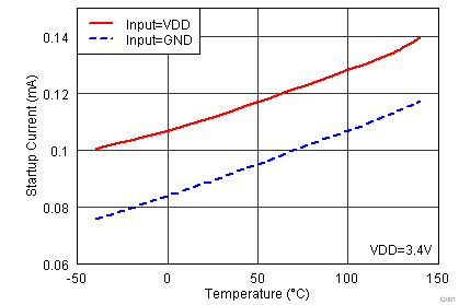
| IDD(off) | Startup current, (based on UCC27524 Input configuration) |
VDD = 3.4 V, INA = VDD, INB = VDD | 55 | 110 | 175 | μA |
| VDD = 3.4 V, INA = GND, INB = GND | 25 | 75 | 145 | |||
| UNDER VOLTAGE LOCKOUT (UVLO) | ||||||
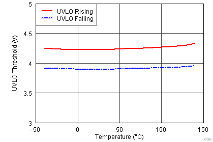
| VON | Supply start threshold | TJ = 25 °C | 3.91 | 4.2 | 4.5 | V |
| TJ = –40 °C to 140 °C | 3.7 | 4.2 | 4.65 | |||
| VOFF | Minimum operating voltage after supply start | 3.4 | 3.9 | 4.4 | V | |
| VDD_H | Supply voltage hysteresis | 0.2 | 0.3 | 0.5 | V | |
| INPUTS (INA, INB, INA+, INA–, INB+, INB–), UCC27524A1-Q1 (DGN) | ||||||
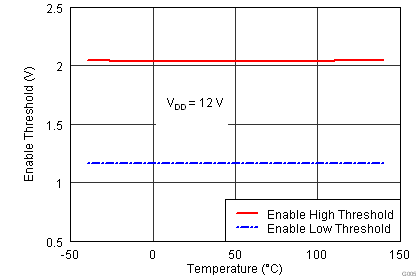
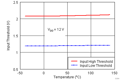
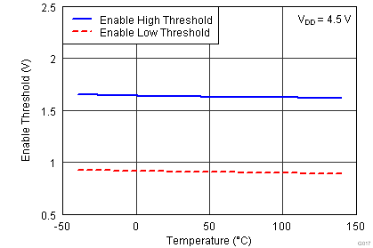
| VIN_H | Input signal high threshold | Output high for non-inverting input pins Output low for inverting input pins |
1.9 | 2.1 | 2.3 | V |
| VIN_L | Input signal low threshold | Output low for non-inverting input pins Output high for inverting input pins |
1 | 1.2 | 1.4 | V |
| VIN_HYS | Input hysteresis | 0.7 | 0.9 | 1.1 | V | |
| OUTPUTS (OUTA, OUTB) | ||||||
| ISNK/SRC | Sink/source peak current(1) | CLOAD = 0.22 µF, FSW = 1 kHz | ±5 | A | ||
| VDD-VOH | High output voltage | IOUT = –10 mA | 0.075 | V | ||
| VOL | Low output voltage | IOUT = 10 mA | 0.01 | V | ||
| ROH | Output pullup resistance(2) | IOUT = –10 mA | 2.5 | 5 | 7.5 | Ω |
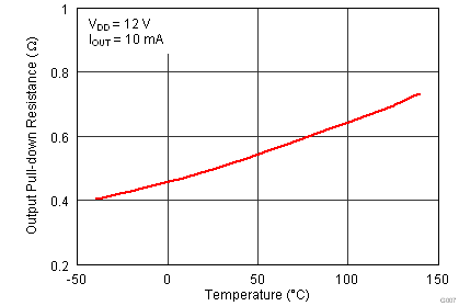
| ROL | Output pulldown resistance | IOUT = 10 mA | 0.15 | 0.5 | 1 | Ω |
(1) Ensured by design.
(2) ROH represents on-resistance of only the P-Channel MOSFET device in the pullup structure of the UCC27524A1-Q1 output stage.
7.6 Switching Characteristics
over operating free-air temperature range (unless otherwise noted)| PARAMETER | TEST CONDITIONS | MIN | TYP | MAX | UNIT | |
|---|---|---|---|---|---|---|
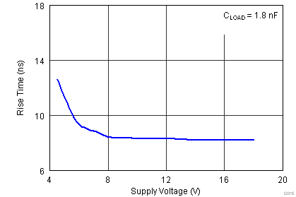
| tR | Rise time(1) | CLOAD = 1.8 nF | 7 | 18 | ns | |
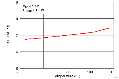
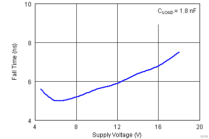
| tF | Fall time(1) | CLOAD = 1.8 nF | 6 | 10 | ns | |
| tM | Delay matching between 2 channels | INA = INB, OUTA and OUTB at 50% transition point | 1 | 4 | ns | |
| tPW | Minimum input pulse width that changes the output state | 15 | 25 | ns | ||
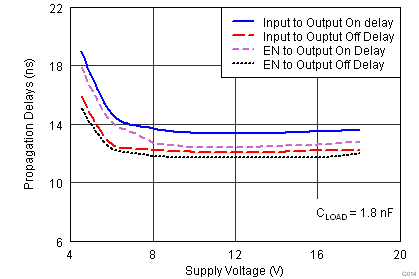
| tD1, tD2 | Input to output propagation delay(1) | CLOAD = 1.8 nF, 5-V input pulse | 6 | 13 | 23 | ns |
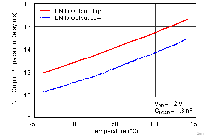
| tD3, tD4 | EN to output propagation delay(1) | CLOAD = 1.8 nF, 5-V enable pulse | 6 | 13 | 23 | ns |
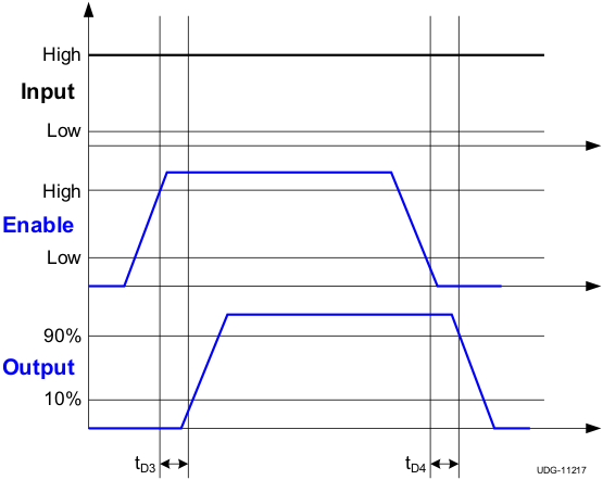 Figure 1. Enable Function
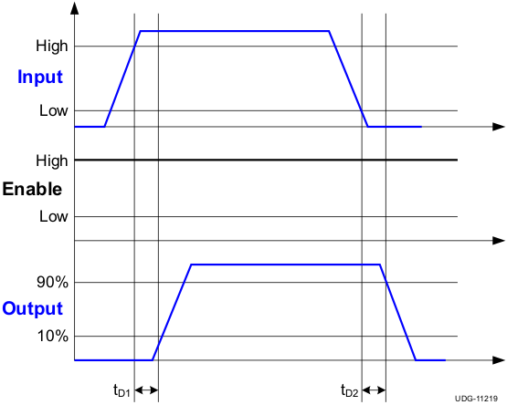 Figure 2. Input-Output Operation
7.7 Typical Characteristics
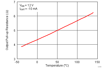
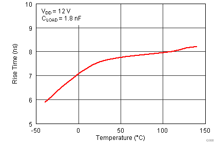
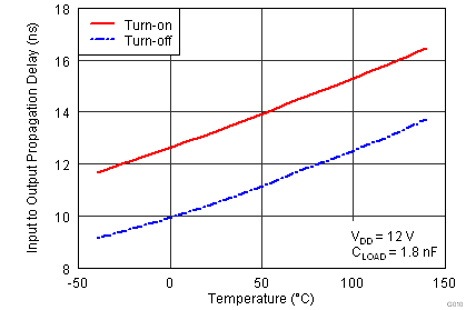
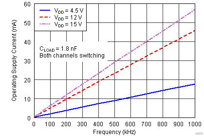
(Outputs Switching)
