SLUSAQ3H November 2011 – June 2024 UCC27523 , UCC27525 , UCC27526
PRODUCTION DATA
- 1
- 1 Features
- 2 Applications
- 3 Description
- 4 Description (continued)
- 5 Pin Configuration and Functions
- 6 Specifications
- 7 Detailed Description
- 8 Application and Implementation
- 9 Power Supply Recommendations
- 10Layout
- 11Device and Documentation Support
- 12Revision History
- 13Mechanical, Packaging, and Orderable Information
パッケージ・オプション
メカニカル・データ(パッケージ|ピン)
サーマルパッド・メカニカル・データ
発注情報
6.7 Typical Characteristics
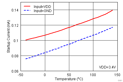 Figure 6-5 Start-Up Current vs Temperature
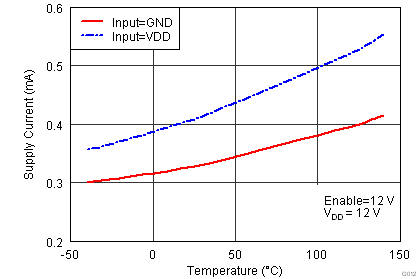 Figure 6-7 Supply Current vs Temperature (Outputs in DC ON/OFF Condition)
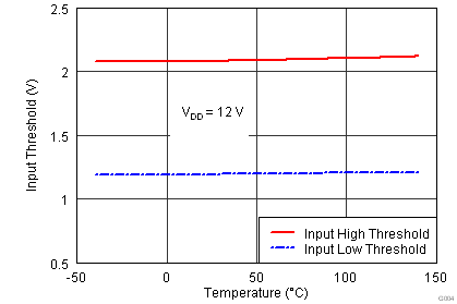 Figure 6-9 Input Threshold vs Temperature
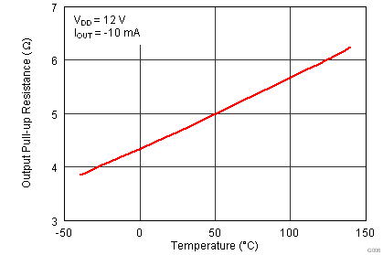 Figure 6-11 Output Pullup Resistance vs Temperature
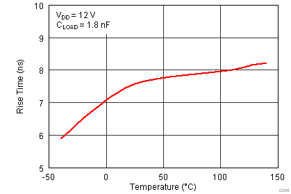 Figure 6-13 Rise Time vs Temperature
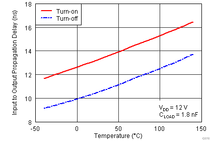 Figure 6-15 Input to Output Propagation Delay vs Temperature
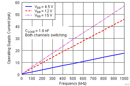 Figure 6-17 Operating Supply Current vs Frequency
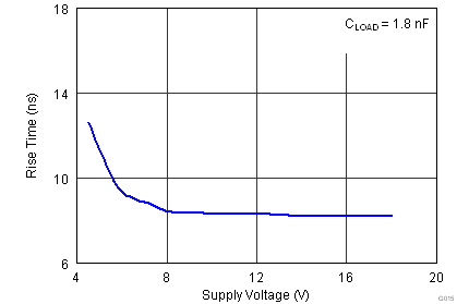 Figure 6-19 Rise Time vs Supply Voltage
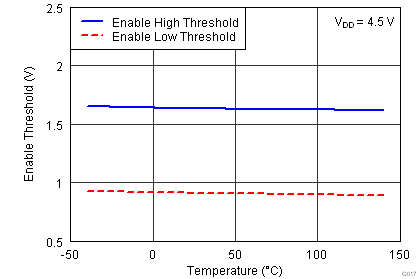 Figure 6-21 Enable Threshold vs Temperature
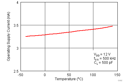 Figure 6-6 Operating Supply Current vs Temperature (Outputs Switching)
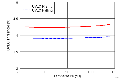 Figure 6-8 UVLO Threshold vs Temperature
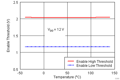 Figure 6-10 Enable Threshold vs Temperature
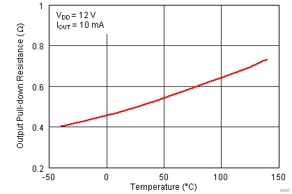 Figure 6-12 Output Pulldown Resistance vs Temperature
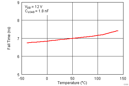 Figure 6-14 Fall Time vs Temperature
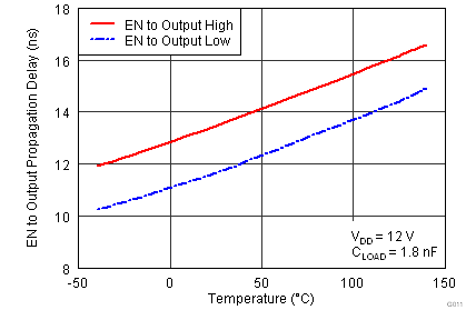 Figure 6-16 EN to Output Propagation Delay vs Temperature
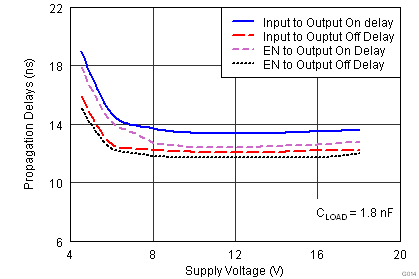 Figure 6-18 Propagation Delays vs Supply Voltage
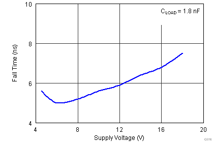 Figure 6-20 Fall Time vs Supply Voltage