JAJSVF6C December   2013  – September 2024 UCC27532-Q1

PRODUCTION DATA  

  1.   1
  2. 特長
  3. アプリケーション
  4. 概要
  5. 概要 (続き)
  6. Pin Configuration and Functions
  7. Specifications
    1. 6.1 Absolute Maximum Ratings
    2. 6.2 ESD Ratings
    3. 6.3 Recommended Operating Conditions
    4. 6.4 Thermal Information
    5. 6.5 Electrical Characteristics
    6. 6.6 Switching Characteristics
    7. 6.7 Typical Characteristics
  8. Detailed Description
    1. 7.1 Overview
    2. 7.2 Functional Block Diagram
    3. 7.3 Feature Description
      1. 7.3.1 VDD Undervoltage Lockout
      2. 7.3.2 Input Stage
      3. 7.3.3 Enable Function
      4. 7.3.4 Output Stage
    4. 7.4 Device Functional Modes
  9. Application and Implementation
    1. 8.1 Application Information
    2. 8.2 Typical Applications
      1. 8.2.1 Driving IGBT Without Negative Bias
        1. 8.2.1.1 Design Requirements
        2. 8.2.1.2 Detailed Design Procedure
          1. 8.2.1.2.1 Input-to-Output Configuration
          2. 8.2.1.2.2 Input Threshold Type
          3. 8.2.1.2.3 VDD Bias Supply Voltage
          4. 8.2.1.2.4 Peak Source and Sink Currents
          5. 8.2.1.2.5 Enable and Disable Function
          6. 8.2.1.2.6 Propagation Delay
          7. 8.2.1.2.7 Power Dissipation
        3. 8.2.1.3 Application Curves
      2. 8.2.2 Driving IGBT With 13-V Negative Turnoff Bias
      3. 8.2.3 Using UCC27532-Q1 Drivers in an Inverter
  10. Power Supply Recommendations
  11. 10Layout
    1. 10.1 Layout Guidelines
    2. 10.2 Layout Example
    3. 10.3 Thermal Consideration
  12. 11Device and Documentation Support
    1. 11.1 サード・パーティ製品に関する免責事項
    2. 11.2 Documentation Support
      1. 11.2.1 Related Documentation
    3. 11.3 ドキュメントの更新通知を受け取る方法
    4. 11.4 サポート・リソース
    5. 11.5 Trademarks
    6. 11.6 静電気放電に関する注意事項
    7. 11.7 用語集
  13. 12Revision History
  14. 13Mechanical, Packaging, and Orderable Information

パッケージ・オプション

メカニカル・データ(パッケージ|ピン)
サーマルパッド・メカニカル・データ
発注情報

VDD Undervoltage Lockout

The UCC27532-Q1 device has an internal undervoltage-lockout (UVLO) protection feature on the VDD-pin supply-circuit blocks. To ensure acceptable power dissipation in the power switch, this UVLO prevents the operation of the gate driver at low supply voltages. Whenever the driver is in UVLO condition (when the VDD voltage less than VON during power up and when the VDD voltage is less than VOFF during power down), this circuit holds all outputs LOW, regardless of the status of the inputs. The UVLO is typically 8.9 V with a 700-mV typical hysteresis. This hysteresis helps prevent chatter when low-VDD supply voltages have noise from the power supply. This hysteresis also prevents chatter when there are droops in the VDD bias voltage when the system commences switching and there is a sudden increase in IDD. The capability to operate at voltage levels such as 10 V to 32 V provides flexibility to drive Si MOSFETs, IGBTs, and emerging SiC FETs.
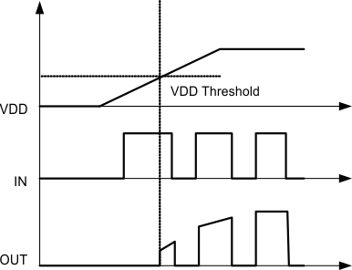
UCC27532-Q1 Power UpFigure 7-1 Power Up