JAJSDL2A August 2017 – August 2018 UCC27712-Q1
PRODUCTION DATA.
- 1 特長
- 2 アプリケーション
- 3 概要
- 4 改訂履歴
- 5 概要(続き)
- 6 Pin Configuration and Functions
- 7 Specifications
- 8 Detailed Description
-
9 Application and Implementation
- 9.1 Application Information
- 9.2
Typical Application
- 9.2.1 Design Requirements
- 9.2.2
Detailed Design Procedure
- 9.2.2.1 Selecting HI and LI Low Pass Filter Components (RHI, RLI, CHI, CLI)
- 9.2.2.2 Selecting Bootstrap Capacitor (CBOOT)
- 9.2.2.3 Selecting VDD Bypass/Holdup Capacitor (CVDD) and Rbias
- 9.2.2.4 Selecting Bootstrap Resistor (RBOOT)
- 9.2.2.5 Selecting Gate Resistor RON/ROFF
- 9.2.2.6 Selecting Bootstrap Diode
- 9.2.2.7 Estimate the UCC27712-Q1 Power Losses (PUCC27712-Q1)
- 9.2.2.8 Estimating Junction Temperature
- 9.2.2.9 Operation With IGBT's
- 9.2.3 Application Curves
- 10Power Supply Recommendations
- 11Layout
- 12デバイスおよびドキュメントのサポート
- 13メカニカル、パッケージ、および注文情報
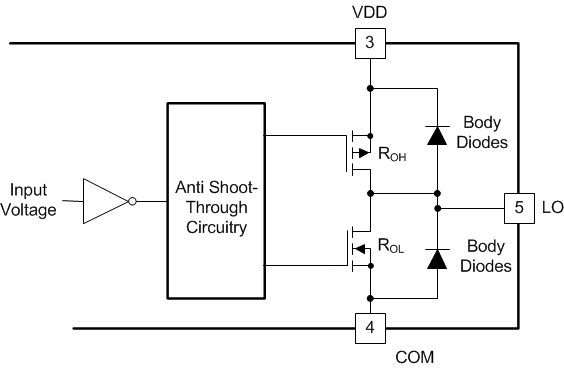
8.3.4 Output Stage
The UCC27712-Q1 device output stage pull-up structure features a P-Channel MOSFET to provide source current until the output is saturated to VDD or HB. The ROH parameter (see Figure 21) is a DC measurement and it is representative of the on-resistance of the P-Channel device.
The pull-down structure in UCC27712-Q1 is composed of a N-Channel MOSFET. The ROL parameter (see Figure 19), which is also a DC measurement, is representative of the impedance of the pull-down stage in the device.
Each output stage in UCC27712-Q1 is capable of supplying 1.8-A peak source and 2.8-A peak sink current pulses. The output voltage swings between (VDD and COM) / (HB and HS) providing rail-to-rail operation, thanks to the MOSFET output stage which delivers very low drop-out.
 Figure 32. Output Stage Structure