JAJSC44B August 2015 – March 2017 UCC27714
PRODUCTION DATA.
- 1 特長
- 2 アプリケーション
- 3 概要
- 4 改訂履歴
- 5 Pin Configuration and Functions
- 6 Specifications
- 7 Detailed Description
-
8 Application and Implementation
- 8.1 Application Information
- 8.2
Typical Application
- 8.2.1 Design Requirements
- 8.2.2
Detailed Design Procedure
- 8.2.2.1 Selecting HI and LI Low Pass Filter Components (RHI, RLI, CHI, CLI)
- 8.2.2.2 Selecting Bootstrap Capacitor (CBOOT)
- 8.2.2.3 Selecting VDD Bypass/Holdup Capacitor (CVDD) and Rbias
- 8.2.2.4 Selecting Bootstrap Resistor (RBOOT)
- 8.2.2.5 Selecting Gate Resistor RHO/RLO
- 8.2.2.6 Selecting Bootstrap Diode
- 8.2.2.7 Estimate the UCC27714 Power Losses (PUCC27714)
- 8.2.2.8 Application Example Schematic Note
- 8.2.2.9 LO and HO Overshoot and Undershoot
- 8.2.3 Application Curves
- 9 Power Supply Recommendations
- 10Layout
- 11デバイスおよびドキュメントのサポート
- 12メカニカル、パッケージ、および注文情報
10 Layout
10.1 Layout Guidelines
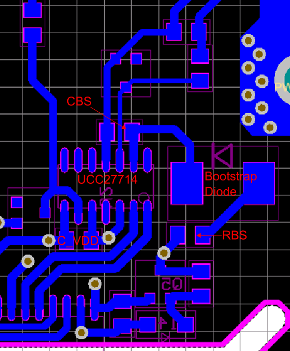
- Locate UCC27714 as close as possible to the MOSFETs in order to minimize the length of high-current traces between the HO/LO and the Gate of MOSFETs.
- A 5-Ω resistor series with bias supply and VDD pin is recommended.
- Locate the VDD capacitor (C_VDD) and VHB capacitor (CBS) as close as possible to the pins of UCC27714.
- A 2-Ω to 5-Ω resistor series with bootstrap diode is recommended to limit bootstrap current.
- A RC filter with 5.1 Ω to 51 Ω and 220 pF for HI/LI is recommended.
- Separate power traces and signal traces, such as output and input signals.
10.2 Layout Example
 Figure 62. UCC27714 Layout Example