SLUS270G March 1999 – May 2020 UCC2800 , UCC2801 , UCC2802 , UCC2803 , UCC2804 , UCC2805
PRODUCTION DATA
- 1 Features
- 2 Applications
- 3 Description
- 4 Revision History
- 5 Description (continued)
- 6 Device Comparison Table
- 7 Pin Configuration and Functions
- 8 Specifications
-
9 Detailed Description
- 9.1 Overview
- 9.2 Functional Block Diagram
- 9.3
Feature Description
- 9.3.1 Detailed Pin Description
- 9.3.2 Undervoltage Lockout (UVLO)
- 9.3.3 Self-Biasing, Active Low Output
- 9.3.4 Reference Voltage
- 9.3.5 Oscillator
- 9.3.6 Synchronization
- 9.3.7 PWM Generator
- 9.3.8 Minimum Off-Time Setting (Dead-Time Control)
- 9.3.9 Leading Edge Blanking
- 9.3.10 Minimum Pulse Width
- 9.3.11 Current Limiting
- 9.3.12 Overcurrent Protection and Full Cycle Restart
- 9.3.13 Soft Start
- 9.3.14 Slope Compensation
- 9.4 Device Functional Modes
- 10Application and Implementation
- 11Power Supply Recommendations
- 12Layout
- 13Device and Documentation Support
- 14Mechanical, Packaging, and Orderable Information
パッケージ・オプション
メカニカル・データ(パッケージ|ピン)
サーマルパッド・メカニカル・データ
発注情報
8.6 Typical Characteristics
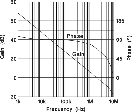 Figure 8-1 Error Amplifier Gain and Phase Response
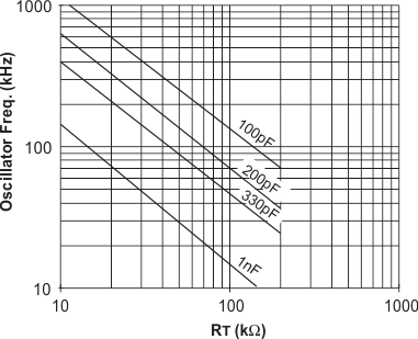 Figure 8-3 UCC2800, UCC2801, UCC2802, and UCC2804 Oscillator Frequency vs RT and CT
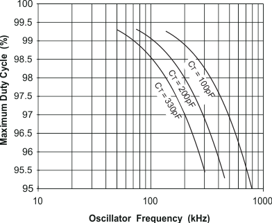 Figure 8-5 UCC2800, UCC2802, and UCC2803 Maximum Duty Cycle vs Oscillator Frequency
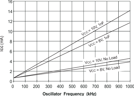 Figure 8-7 UCC2800 ICC vs Oscillator Frequency
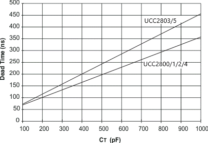 Figure 8-9 Dead Time vs CT, RT = 100 k
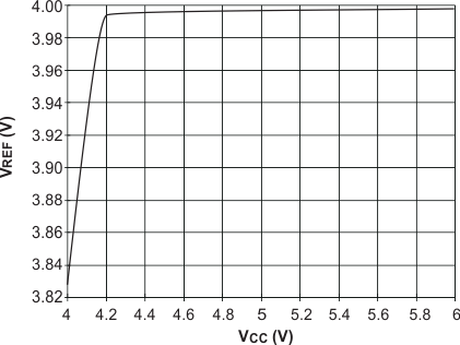 Figure 8-2 UCC2803 and UCC2805VREF vs VCC, ILOAD = 0.5 mA
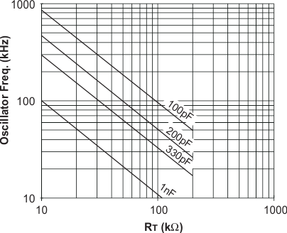 Figure 8-4 UCC2803 and UCC2805 Oscillator Frequency vs RT and CT
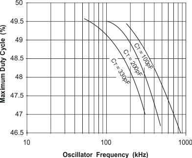 Figure 8-6 UCC2801, UCC2804, and UCC2805 Maximum Duty Cycle vs Oscillator Frequency
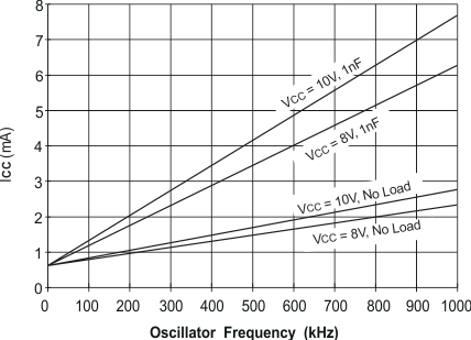 Figure 8-8 UCC2805 ICC vs Oscillator Frequency
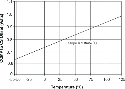 Figure 8-10 COMP to CS Offset vs Temperature, CS = 0 V