JAJSC34B March 2012 – December 2023 UCC28070A
PRODUCTION DATA
- 1
- 1 特長
- 2 アプリケーション
- 3 概要
- 4 Pin Configuration and Functions
- 5 Specifications
-
6 Detailed Description
- 6.1 Overview
- 6.2 Functional Block Diagram
- 6.3
Feature Description
- 6.3.1 Interleaving
- 6.3.2 Programming the PWM Frequency and Maximum Duty-Cycle Clamp
- 6.3.3 Frequency Dithering (Magnitude and Rate)
- 6.3.4 External Clock Synchronization
- 6.3.5 Multi-phase Operation
- 6.3.6 VSENSE and VINAC Resistor Configuration
- 6.3.7 VSENSE and VINAC Open-Circuit Protection
- 6.3.8 Current Synthesizer
- 6.3.9 Programmable Peak Current Limit
- 6.3.10 Linear Multiplier and Quantized Voltage Feed Forward
- 6.3.11 Enhanced Transient Response (VA Slew-Rate Correction)
- 6.3.12 Voltage Biasing (VCC and VVREF)
- 6.3.13 PFC Enable and Disable
- 6.3.14 Adaptive Soft Start
- 6.3.15 PFC Start-Up Hold Off
- 6.3.16 Output Overvoltage Protection (OVP)
- 6.3.17 Zero-Power Detection
- 6.3.18 Thermal Shutdown
- 6.3.19 Current Loop Compensation
- 6.3.20 Voltage Loop Compensation
- 6.4 Device Functional Modes
-
7 Application and Implementation
- 7.1 Application Information
- 7.2
Typical Application
- 7.2.1 Design Requirements
- 7.2.2
Detailed Design Procedure
- 7.2.2.1 Output Current Calculation
- 7.2.2.2 Bridge Rectifier
- 7.2.2.3 PFC Inductor (L1 and L2)
- 7.2.2.4 PFC MOSFETs (M1 and M2)
- 7.2.2.5 PFC Diode
- 7.2.2.6 PFC Output Capacitor
- 7.2.2.7 Current-Loop Feedback Configuration (Sizing of the Current-Transformer Turns-Ratio and Sense Resistor (RS))
- 7.2.2.8 Current-Sense Offset and PWM Ramp for Improved Noise Immunity
- 7.2.3 Application Curves
- 7.3 Power Supply Recommendations
- 7.4 Layout
- 8 Device and Documentation Support
- 9 Revision History
- 10Mechanical, Packaging, and Orderable Information
5.6 Typical Characteristics
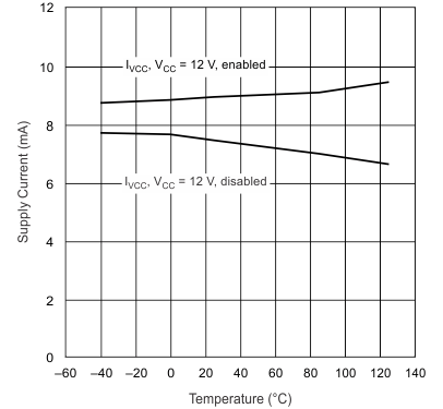 Figure 5-1 VCC
Supply Current vs Junction Temperature
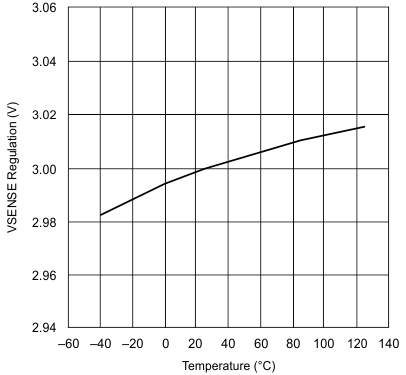 Figure 5-3 VVSENSE Regulation vs Junction Temperature
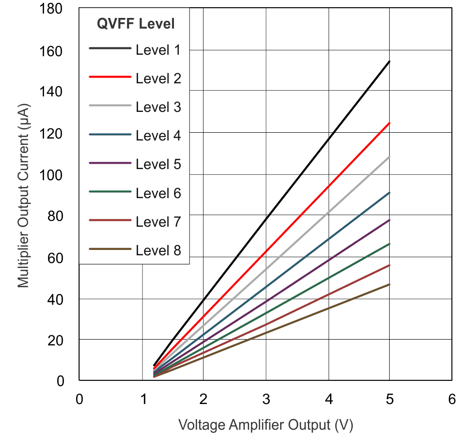 Figure 5-5 IMO,
Multiplier Output Current vs VVAO
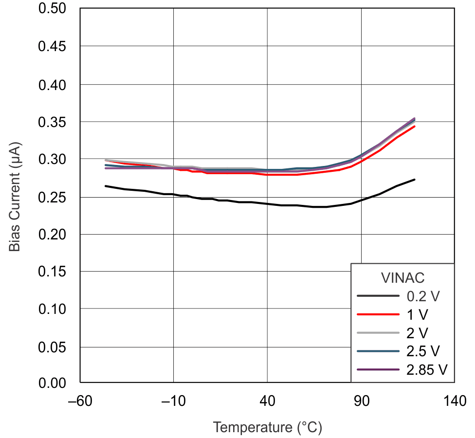 Figure 5-7 IVINAC Bias Current vs Junction Temperature
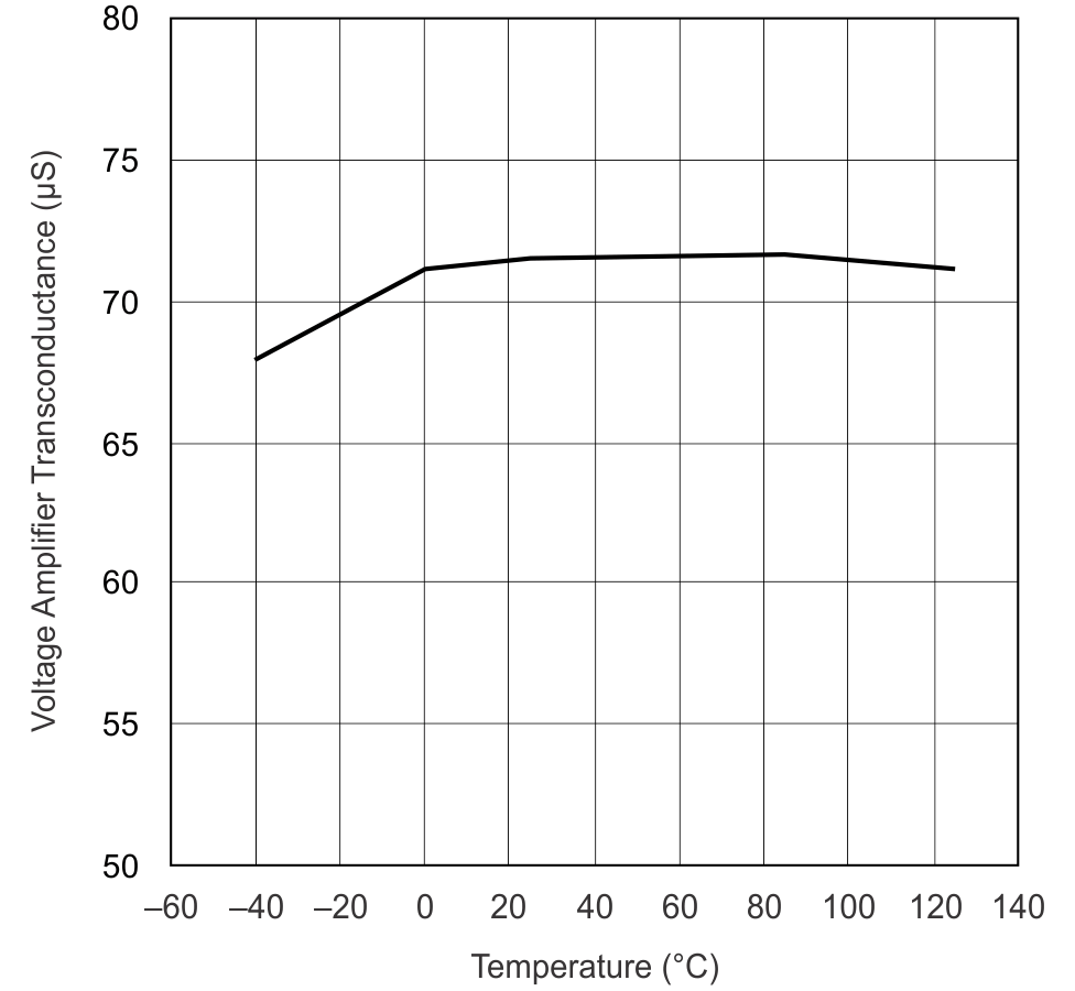 Figure 5-9 VAO,
Voltage Amplifier Transconductance vs Junction Temperature
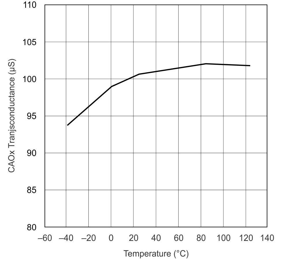 Figure 5-11 Current Amplifier Transconductance vs Junction Temperature
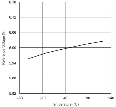
| IVREF = 0mA |
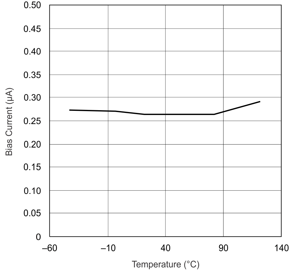 Figure 5-4 IVSENSE Bias Current vs Junction Temperature
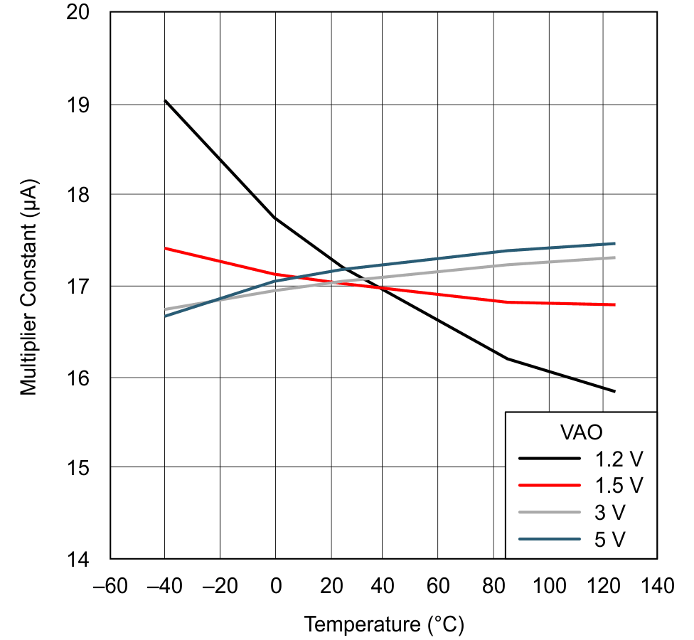 Figure 5-6 Multiplier Constant vs Junction Temperature
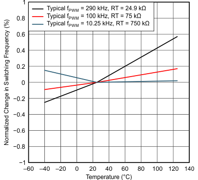 Figure 5-8 Switching Frequency vs Temperature
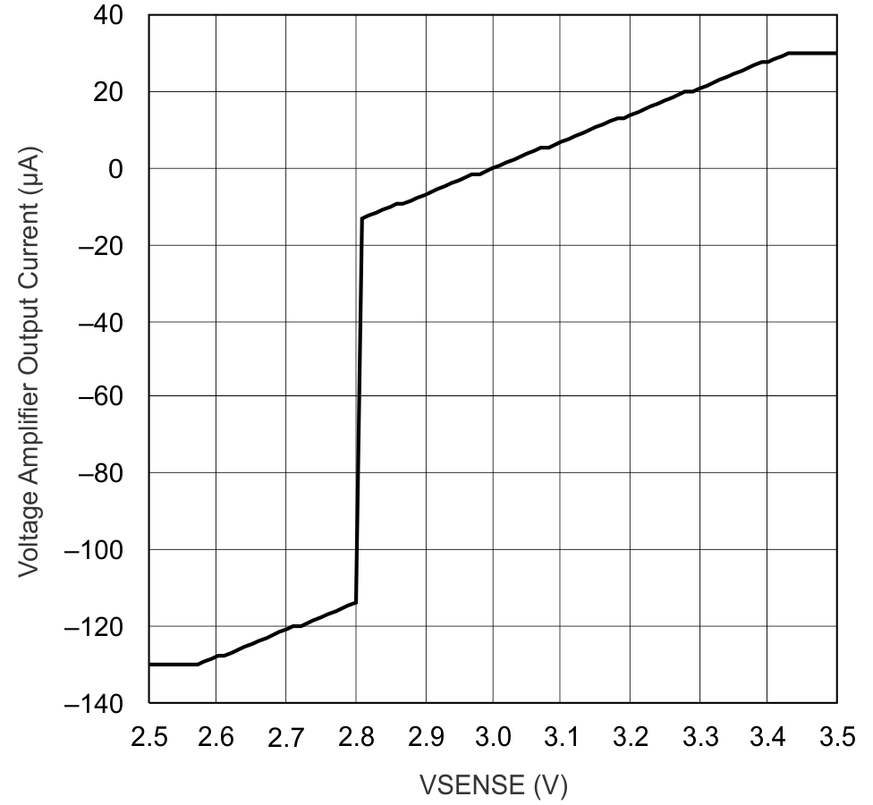 Figure 5-10 Voltage Amplifier Transfer Function vs VVSENSE
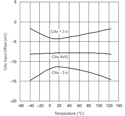
| 0.8V Common Mode | ||
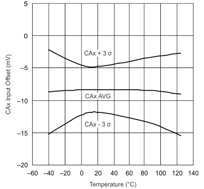
| 2V Common Mode |
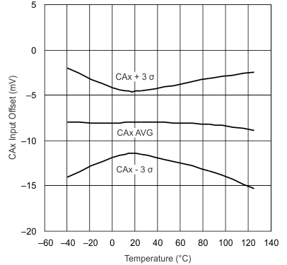
| 3.6V Common Mode | ||

| 0.8V Common Mode | ||
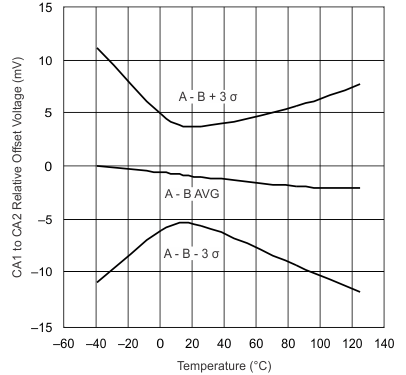
| 2V Common Mode |
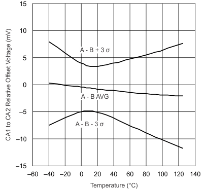
| 3.6V Common Mode | ||