SLUS168E Apr 1999 – August 2015 UCC2808-1 , UCC2808-2 , UCC3808-1 , UCC3808-2
PRODUCTION DATA.
8 Application and Implementation
NOTE
Information in the following applications sections is not part of the TI component specification, and TI does not warrant its accuracy or completeness. TI’s customers are responsible for determining suitability of components for their purposes. Customers should validate and test their design implementation to confirm system functionality.
8.1 Application Information
The UCCx808-x PWM controller contains all of the features needed to implement push-pull topology, using current-mode control in a small 8-pin package. The UCCx808-x is designed for current-mode control push-pull topology. UCCx808-x employs advantages of current-mode control, peak current sense, overcurrent protection.
8.2 Typical Application
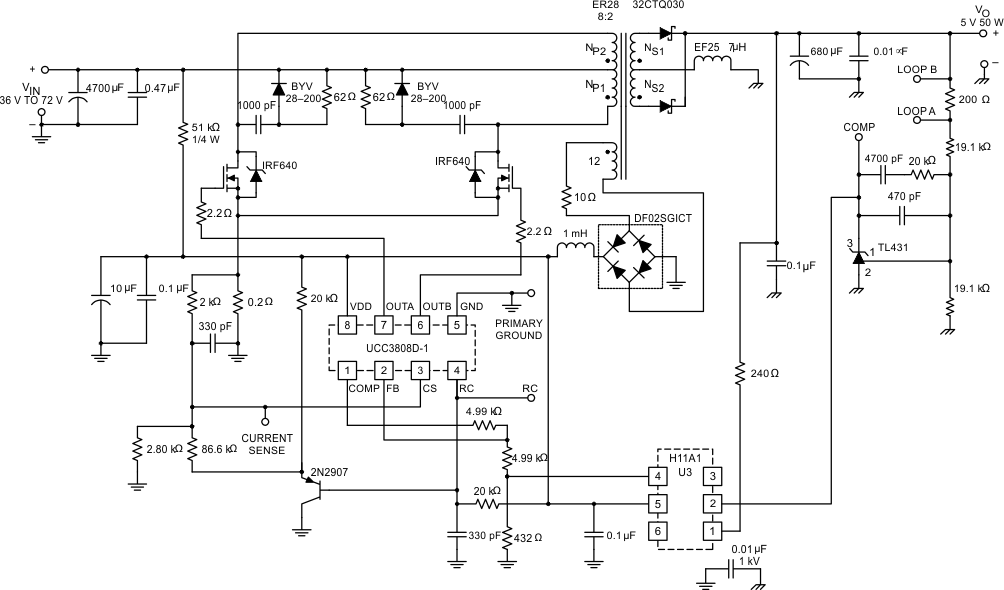
A 200-kHz push-pull application circuit with a full wave rectifier is shown in Figure 6.
 Figure 6. Typical Application Diagram: 48-V In, 5-V, 50-W Output
8.2.1 Design Requirements
Table 3 lists the design parameters of the UCC3808-x.
Table 3. Design Parameters
| DESIGN PARAMETER | TARGET VALUE | |||
|---|---|---|---|---|
| Output voltage | 5 V | |||
| Rated output power | 50 W | |||
| Input DC voltage range | 36 V to 72 V | |||
| Switching frequency | 210 kHz | |||
8.2.2 Detailed Design Procedure
The output, VO, provides 5 V at 75 W maximum and is electrically isolated from the input. Since the UCC3808 is a peak current mode controller the 2N2222A emitter following amplifier (buffers the CT waveform) provides slope compensation which is necessary for duty ratios greater than 50%. Capacitor decoupling is very important with a single ground IC controller, and a 1 μF is suggested as close to the IC as possible. The controller supply is a series RC for start-up, paralleled with a bias winding on the output inductor used in steadystate operation.
Isolation is provided by an optocoupler with regulation done on the secondary side using the UC3965 Precision Reference with Low Offset Error Amplifier. Small signal compensation with tight voltage regulation is achieved using this part on the secondary side. Many choices exist for the output inductor depending on cost, volume, and mechanical strength. Several design options are iron powder, molypermalloy (MPP), or a ferrite core with an air gap as shown here. The main power transformer is a low profile design, EFD size 25, using Magnetics Inc. P material which is a good choice at this frequency and temperature. The input voltage may range from 36 V DC to 72 V DC.
8.2.3 Application Curves
 Figure 7. Error Amplifier Gain and Phase Response vs Frequency
 Figure 8. Dead Time vs Timing Resistor