-
UCC2813-x-Q1 Low-Power Economy BiCMOS Current-Mode PWM SGLS245E May 2020 – May 2020 UCC2813-0-Q1 , UCC2813-1-Q1 , UCC2813-2-Q1 , UCC2813-3-Q1 , UCC2813-4-Q1 , UCC2813-5-Q1
PRODUCTION DATA.
-
UCC2813-x-Q1 Low-Power Economy BiCMOS Current-Mode PWM
- 1 Features
- 2 Applications
- 3 Description
- 4 Revision History
- 5 Device Comparison Table
- 6 Pin Configuration and Functions
- 7 Specifications
-
8 Detailed Description
- 8.1 Overview
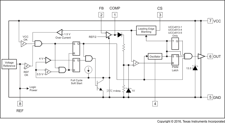
- 8.2 Functional Block Diagram
- 8.3
Feature Description
- 8.3.1 Detailed Pin Descriptions
- 8.3.2 Undervoltage Lockout (UVLO)
- 8.3.3 Self-Biasing, Active Low Output
- 8.3.4 Reference Voltage
- 8.3.5 Oscillator
- 8.3.6 Synchronization
- 8.3.7 PWM Generator
- 8.3.8 Minimum Off-Time Adjustment (Dead-Time Control)
- 8.3.9 Leading Edge Blanking
- 8.3.10 Minimum Pulse Width
- 8.3.11 Current Limiting
- 8.3.12 Overcurrent Protection and Full-Cycle Restart
- 8.3.13 Soft Start
- 8.3.14 Slope Compensation
- 8.4 Device Functional Modes
-
9 Application and Implementation
- 9.1 Application Information
- 9.2
Typical Application
- 9.2.1 Design Requirements
- 9.2.2
Detailed Design Procedure
- 9.2.2.1 Bulk Capacitor Calculation
- 9.2.2.2 Transformer Design
- 9.2.2.3 MOSFET and Output Diode Selection
- 9.2.2.4 Output Capacitor Calculation
- 9.2.2.5 Current Sensing Network
- 9.2.2.6 Gate Drive Resistor
- 9.2.2.7 REF Bypass Capacitor
- 9.2.2.8 RT and CT
- 9.2.2.9 Start-Up Circuit
- 9.2.2.10 Voltage Feedback Compensation Procedure
- 9.2.3 Application Curves
- 10Power Supply Recommendations
- 11Layout
- 12Device and Documentation Support
- 13Mechanical, Packaging, and Orderable Information
- IMPORTANT NOTICE
パッケージ・オプション
デバイスごとのパッケージ図は、PDF版データシートをご参照ください。
メカニカル・データ(パッケージ|ピン)
- D|8
- PW|8
サーマルパッド・メカニカル・データ
発注情報
UCC2813-x-Q1 Low-Power Economy BiCMOS Current-Mode PWM
1 Features
- Qualified for automotive applications
- AEC-Q100 qualified with the following results:
- Device temperature grade 1: –40°C to 125°C TA
- Device HBM classification level 2: ±2 kV
- Device CDM classification level C5: >1000 V
- 100-µA typical starting supply current
- 500-µA typical operating supply current
- Operation to 1 MHz
- Internal soft start
- Internal fault soft start
- Internal leading-edge blanking of the current-sense signal
- 1-A totem-pole output
- 70-ns typical response from current-sense to gate-drive output
- 1.5% tolerance voltage reference
- Same pinout as the UCC3802 device, UC3842 device, and UC3842A device families
2 Applications
- Automotive power supplies
- Auxiliary power supply for automotive hybrid and electric vehicles
- AC and DC power supplies
3 Description
The UCC2813-x-Q1 device family of high-speed, low-power integrated circuits contains all of the control and drive components required for off-line and DC-to-DC fixed-frequency current-mode switching power supplies with minimal parts count.
These devices have the same pin configuration as the UC284x device family, and also offer the added features of internal full-cycle soft start and internal leading-edge blanking of the current-sense input.
The UCC2813-x-Q1 device family offers a variety of package options, choice of maximum duty cycle, and choice of critical voltage levels. Devices with lower reference voltage such as the UCC2813-3-Q1 and UCC2813-5-Q1 fit best into battery operated systems, while the higher reference and the higher UVLO hysteresis of the UCC2813-2-Q1 device and UCC2813-4-Q1 device make these ideal choices for use in off-line power supplies.
The UCC2813-x-Q1 device series is specified for operation from –40°C to 125°C.
Device Information(1)
| PART NUMBER | PACKAGE | BODY SIZE (NOM) |
|---|---|---|
| UCC2813-x-Q1 | SOIC (8) | 3.91 mm × 4.90 mm |
| TSSOP (8) | 4.40 mm × 3.00 mm |
- For all available packages, see the orderable addendum at the end of the data sheet.
Device Images
Block Diagram
