SGLS245E May 2020 – May 2020 UCC2813-0-Q1 , UCC2813-1-Q1 , UCC2813-2-Q1 , UCC2813-3-Q1 , UCC2813-4-Q1 , UCC2813-5-Q1
PRODUCTION DATA.
- 1 Features
- 2 Applications
- 3 Description
- 4 Revision History
- 5 Device Comparison Table
- 6 Pin Configuration and Functions
- 7 Specifications
-
8 Detailed Description
- 8.1 Overview
- 8.2 Functional Block Diagram
- 8.3
Feature Description
- 8.3.1 Detailed Pin Descriptions
- 8.3.2 Undervoltage Lockout (UVLO)
- 8.3.3 Self-Biasing, Active Low Output
- 8.3.4 Reference Voltage
- 8.3.5 Oscillator
- 8.3.6 Synchronization
- 8.3.7 PWM Generator
- 8.3.8 Minimum Off-Time Adjustment (Dead-Time Control)
- 8.3.9 Leading Edge Blanking
- 8.3.10 Minimum Pulse Width
- 8.3.11 Current Limiting
- 8.3.12 Overcurrent Protection and Full-Cycle Restart
- 8.3.13 Soft Start
- 8.3.14 Slope Compensation
- 8.4 Device Functional Modes
-
9 Application and Implementation
- 9.1 Application Information
- 9.2
Typical Application
- 9.2.1 Design Requirements
- 9.2.2
Detailed Design Procedure
- 9.2.2.1 Bulk Capacitor Calculation
- 9.2.2.2 Transformer Design
- 9.2.2.3 MOSFET and Output Diode Selection
- 9.2.2.4 Output Capacitor Calculation
- 9.2.2.5 Current Sensing Network
- 9.2.2.6 Gate Drive Resistor
- 9.2.2.7 REF Bypass Capacitor
- 9.2.2.8 RT and CT
- 9.2.2.9 Start-Up Circuit
- 9.2.2.10 Voltage Feedback Compensation Procedure
- 9.2.3 Application Curves
- 10Power Supply Recommendations
- 11Layout
- 12Device and Documentation Support
- 13Mechanical, Packaging, and Orderable Information
パッケージ・オプション
デバイスごとのパッケージ図は、PDF版データシートをご参照ください。
メカニカル・データ(パッケージ|ピン)
- D|8
- PW|8
サーマルパッド・メカニカル・データ
発注情報
8.3.12 Overcurrent Protection and Full-Cycle Restart
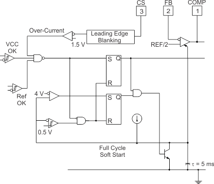
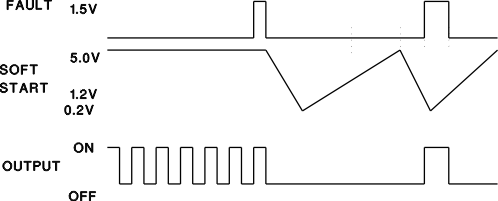
A separate overcurrent comparator within the UCC2813-x-Q1 devices handles operation into a short-circuited or severely overloaded power supply output. This overcurrent comparator has a 1.5-V threshold and is also gated by the leading edge blanking signal to prevent false triggering. Once triggered, the overcurrent comparator uses the internal soft-start capacitor to generate a delay before retry is attempted. Often referred to as hiccup, this delay time is used to significantly reduce the input and dissipated power of the main converter and switching components. Full-cycle soft start ensures that there is a predictable delay of greater than 3 ms between successive attempts to operate during fault conditions. The circuit shown in Figure 28 and the timing diagram in Figure 29 show how the device responds to a severe fault, such as a saturated inductor. When the peak current fault is first detected, the internal soft-start capacitor instantly discharges and stays discharged until the fault clears. At the same time, the PWM output is turned off and held off. When the fault clears, the capacitor slowly charges and allows the error amp output (COMP) to rise. When COMP gets high enough to enable the output, another fault occurs, latching off the PWM output, but the soft-start capacitor still continues to rise to 4 V before being discharged and permitting start of a new cycle. This means that for a severe fault, successive retries is spaced by the time required to fully charge the soft-start capacitor. TI recommends low leakage transformer designs in high-frequency applications to activate the overcurrent protection feature. Otherwise, the switch current may not ramp up sufficiently to trigger the overcurrent comparator within the leading edge blanking duration. This condition would cause continual cyclical triggering of the cycle-by-cycle current limit comparator but not the overcurrent comparator. This would result in brief high power dissipation durations in the main converter at the switching frequency. The intent of the overcurrent comparator is to reduce the effective retry rate under these conditions to a few milliseconds, thus significantly lowering the short-circuit power dissipation of the converter.
 Figure 28. Detailed Block Diagram for Overcurrent Protection
  Figure 29. Device Behavior with Repetitive Fault at CS