SLUS395K February 2000 – October 2015 UCC2817 , UCC2818 , UCC3817 , UCC3818
PRODUCTION DATA.
- 1 Features
- 2 Applications
- 3 Description
- 4 Revision History
- 5 Pin Configuration and Functions
- 6 Specifications
- 7 Detailed Description
- 8 Application and Implementation
- 9 Power Supply Recommendations
- 10Layout
- 11Device and Documentation Support
- 12Mechanical, Packaging, and Orderable Information
パッケージ・オプション
デバイスごとのパッケージ図は、PDF版データシートをご参照ください。
メカニカル・データ(パッケージ|ピン)
- N|16
- DW|16
- D|16
サーマルパッド・メカニカル・データ
- DW|16
発注情報
6 Specifications
6.1 Absolute Maximum Ratings
over operating free-air temperature range (unless otherwise noted) (1)| MIN | MAX | UNIT | ||
|---|---|---|---|---|
| Supply voltage VCC | 18 | V | ||
| Supply current ICC | 20 | mA | ||
| Gate drive current, continuous | 0.2 | A | ||
| Gate drive current | 1.2 | A | ||
| Input voltage, CAI, MOUT, SS | 8 | V | ||
| Input voltage, PKLMT | 5 | V | ||
| Input voltage, VSENSE, OVP/EN | 10 | V | ||
| Input current, RT, IAC, PKLMT | 10 | mA | ||
| Input current, VCC (no switching) | 20 | mA | ||
| Maximum negative voltage, DRVOUT, PKLMT, MOUT | –0.5 | V | ||
| Power dissipation | 1 | W | ||
| TJ | Junction temperature | –55 | 150 | °C |
| Tstg | Storage temperature | –65 | 150 | °C |
| Tsol | Lead temperature (soldering, 10 seconds) | 300 | °C | |
(1) Stresses beyond those listed under Absolute Maximum Ratings may cause permanent damage to the device. These are stress ratings only, which do not imply functional operation of the device at these or any other conditions beyond those indicated under Recommended Operating Conditions. Exposure to absolute-maximum-rated conditions for extended periods may affect device reliability.
6.2 ESD Ratings
| VALUE | UNIT | |||
|---|---|---|---|---|
| V(ESD) | Electrostatic discharge | Human-body model (HBM), per ANSI/ESDA/JEDEC JS-001(1) | ±2000 | V |
| Charged-device model (CDM), per JEDEC specification JESD22-C101(2) | ±1500 | |||
(1) JEDEC document JEP155 states that 500-V HBM allows safe manufacturing with a standard ESD control process.
(2) JEDEC document JEP157 states that 250-V CDM allows safe manufacturing with a standard ESD control process.
6.3 Recommended Operating Conditions
over operating free-air temperature range (unless otherwise noted)| MIN | NOM | MAX | UNIT | ||
|---|---|---|---|---|---|
| VCC | Input voltage | 12 | V | ||
| VSENSE | Input sense voltage | 7.5 | 10 | V | |
| Input current for oscillator | 1.36 | 10 | mA | ||
6.4 Thermal Information
| THERMAL METRIC(1) | UCC281x, UCC381x | UNIT | ||||
|---|---|---|---|---|---|---|
| SOIC (D) | SOIC (DW) | PDIP (N) | TSSOP (PW) | |||
| 16 PINS | 16 PINS | 16 PINS | 16 PINS | |||
| RθJA | Junction-to-ambient thermal resistance | 73.9(2) | 74.1(2) | 49.3(2) | 98.9(3) | °C/W |
| RθJC(top) | Junction-to-case (top) thermal resistance | 33.5 | 35.5 | 38.9 | 30.2(3) | °C/W |
| RθJB | Junction-to-board thermal resistance | 31.4 | 38.9 | 29.4 | 44.8 | °C/W |
| ψJT | Junction-to-top characterization parameter | 5.8 | 9.9 | 18.9 | 1.9 | °C/W |
| ψJB | Junction-to-board characterization parameter | 31.1 | 38.3 | 29.2 | 44.1 | °C/W |
(1) For more information about traditional and new thermal metrics, For more information about traditional and new thermal metrics, see the Semiconductor and IC Package Thermal Metrics application report.
(2) Specified θja (junction to ambient) is for devices mounted to 5-inch2 FR4 PC board with one ounce copper, where noted. When resistance range is given, lower values are for 5 inch2 aluminum PC board. Test PWB was 0.062-inch thick and typically used 0.635-mm trace widths for power packages and 1.3-mm trace widths for non-power packages with a 100-mil × 100-mil probe land area at the end of each trace.
(3) Modeled data. If value range given for θja, lower value is for 3×3 inch. 1 oz internal copper ground plane, higher value is for 1×1-inch. ground plane. All model data assumes only one trace for each non-fused lead.
6.5 Electrical Characteristics
TA = 0°C to 70°C for the UCC3817, and TA = −40°C to 85°C for the UCC2817, TA = TJ, VCC = 12 V, RT = 22 kΩ, CT = 270 pF, (unless otherwise noted)| PARAMETER | TEST CONDITIONS | MIN | TYP | MAX | UNIT | |
|---|---|---|---|---|---|---|
| SUPPLY CURRENT | ||||||
| Supply current, off | VCC = (VCC turn-on threshold −0.3 V) | 150 | 300 | µA | ||
| Supply current, on | VCC = 12 V, No load on DRVOUT | 2 | 4 | 6 | mA | |
| UVLO | ||||||
| VCC turn-on threshold (UCCx817) | 15.4 | 16 | 16.6 | V | ||
| VCC turn-off threshold (UCCx817) | 9.4 | 9.7 | V | |||
| UVLO hysteresis (UCCx817) | 5.8 | 6.3 | V | |||
| Maximum shunt voltage (UCCx817) | IVCC = 10 mA | 15.4 | 17 | 17.5 | V | |
| VCC turn-on threshold (UCCx818) | 9.7 | 10.2 | 10.8 | V | ||
| VCC turn-off threshold (UCCx818) | 9.4 | 9.7 | V | |||
| UVLO hysteresis (UCCx818) | 0.3 | 0.5 | V | |||
| VOLTAGE AMPLIFIER | ||||||
| Input voltage | TA = 0°C to 70°C | 7.387 | 7.5 | 7.613 | V | |
| TA = −40°C to 85°C | 7.369 | 7.5 | 7.631 | |||
| VSENSE bias current | VSENSE = VREF, VAOUT = 2.5 V | 50 | 200 | nA | ||
| Open loop gain | VAOUT = 2 V to 5 V | 50 | 90 | dB | ||
| High-level output voltage | IL = −150 μA | 5.3 | 5.5 | 5.6 | V | |
| Low-level output voltage | IL = 150 μA | 0 | 50 | 150 | mV | |
| OVERVOLTAGE PROTECTION AND ENABLE | ||||||
| Over voltage reference | VREF +0.48 | VREF +0.50 | VREF +0.52 | V | ||
| Hysteresis | 300 | 500 | 600 | mV | ||
| Enable threshold | 1.7 | 1.9 | 2.1 | V | ||
| Enable hysteresis | 0.1 | 0.2 | 0.3 | V | ||
| CURRENT AMPLIFIER | ||||||
| Input offset voltage | VCM = 0 V, VCAOUT = 3 V | –3.5 | 0 | 2.5 | mV | |
| Input bias current | VCM = 0 V, VCAOUT = 3 V | –50 | –100 | nA | ||
| Input offset current | VCM = 0 V, VCAOUT = 3 V | 25 | 100 | nA | ||
| Open loop gain | VCM = 0 V, VCAOUT = 2 V to 5 V | 90 | dB | |||
| Common-mode rejection ratio | VCM = 0 V to 1.5 V, VCAOUT = 3 V | 60 | 80 | dB | ||
| High-level output voltage | IL = −120 μA | 5.6 | 6.5 | 6.8 | V | |
| Low-level output voltage | IL = 1 mA | 0.1 | 0.2 | 0.5 | V | |
| Gain bandwidth product | (1) | 2.5 | MHz | |||
| VOLTAGE REFERENCE | ||||||
| Input voltage | TA = 0°C to 70°C | 7.387 | 7.5 | 7.613 | V | |
| TA = −40°C to 85°C | 7.369 | 7.5 | 7.631 | |||
| Load regulation | IREF = 1 mA to 2 mA | 0 | 10 | mV | ||
| Line regulation | VCC = 10.8 V to 15 V, (2) | 0 | 10 | mV | ||
| Short-circuit current | VREF = 0 V | –20 | –25 | –50 | mA | |
| OSCILLATOR | ||||||
| Initial accuracy | TA = 25°C | 85 | 100 | 115 | kHz | |
| Voltage stability | VCC = 10.8 V to 15 V | –1% | 1% | |||
| Total variation | Line, temp | 80 | 120 | kHz | ||
| Ramp peak voltage | 4.5 | 5 | 5.5 | V | ||
| Ramp amplitude voltage (peak to peak) | 3.5 | 4 | 4.5 | V | ||
| PEAK CURRENT LIMIT | ||||||
| PKLMT reference voltage | –15 | 15 | mV | |||
| PKLMT propagation delay | 150 | 350 | 500 | ns | ||
| MULTIPLIER | ||||||
| IMOUT, high line, low power output current, (0°C to 85°C) | IAC = 500 μA, VFF = 4.7 V, VAOUT = 1.25 V | 0 | –6 | –20 | µA | |
| IMOUT, high line, low power output current, (–40°C to 85°C) | IAC = 500 μA, VFF = 4.7 V, VAOUT = 1.25 V | 0 | –6 | –23 | µA | |
| IMOUT, high line, high power output current | IAC = 500 μA, VFF = 4.7 V, VAOUT = 5 V | –70 | –90 | –105 | µA | |
| IMOUT, low line, low power output current | IAC = 150 μA, VFF = 1.4 V, VAOUT = 1.25 V | –10 | –19 | –50 | µA | |
| IMOUT, low line, high power output current | IAC = 150 μA, VFF = 1.4 V, VAOUT = 5 V | –268 | –300 | –345 | µA | |
| IMOUT, IAC limited output current | IAC = 150 μA, VFF = 1.3 V, VAOUT = 5 V | –250 | –300 | –400 | µA | |
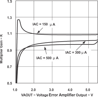
| Gain constant (K) | IAC = 300 μA, VFF = 3 V, VAOUT = 2.5 V | 0.5 | 1 | 1.5 | 1/V | |
| IMOUT, zero current | IAC = 150 μA, VFF = 1.4 V, VAOUT = 0.25 V | 0 | –2 | µA | ||
| IAC = 500 μA, VFF = 4.7 V, VAOUT = 0.25 V | 0 | –2 | ||||
| IMOUT, zero current, (0°C to 85°C) | IAC = 500 μA, VFF = 4.7 V, VAOUT = 0.5 V | 0 | –3 | µA | ||
| IMOUT, zero current, (–40°C to 85°C) | IAC = 500 μA, VFF = 4.7 V, VAOUT = 0.5 V | 0 | –3.5 | µA | ||
| Power limit (IMOUT x VFF) | IAC = 150 μA, VFF = 1.4 V, VAOUT = 5 V | –375 | –420 | –485 | µW | |
| FEED-FORWARD | ||||||
| VFF output current | IAC = 300 μA | –140 | –150 | –160 | µA | |
| SOFT START | ||||||
| SS charge current | –6 | –10 | –16 | µA | ||
| GATE DRIVER | ||||||
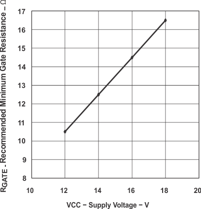
| Pullup resistance | IO = –100 mA to −200 mA | 5 | 12 | Ω | ||
| Pulldown resistance | IO = 100 mA | 2 | 10 | Ω | ||
| Output rise time | CL = 1 nF, RL = 10 Ω, VDRVOUT = 0.7 V to 9.0 V | 25 | 50 | ns | ||
| Output fall time | CL = 1 nF, RL = 10 Ω, VDRVOUT = 9.0 V to 0.7 V | 10 | 50 | ns | ||
| Maximum duty cycle | 93% | 95% | 99% | |||
| Minimum controlled duty cycle | At 100 kHz | 2% | ||||
| ZERO POWER | ||||||
| Zero power comparator threshold | Measured on VAOUT | 0.20 | 0.33 | 0.50 | V | |
(1) Ensured by design, not production tested.
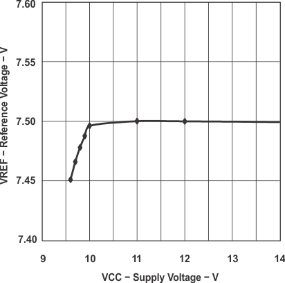
(2) Reference variation for VCC < V is shown in Figure 1.
6.6 Typical Characteristics
