SLUS395K February 2000 – October 2015 UCC2817 , UCC2818 , UCC3817 , UCC3818
PRODUCTION DATA.
- 1 Features
- 2 Applications
- 3 Description
- 4 Revision History
- 5 Pin Configuration and Functions
- 6 Specifications
- 7 Detailed Description
- 8 Application and Implementation
- 9 Power Supply Recommendations
- 10Layout
- 11Device and Documentation Support
- 12Mechanical, Packaging, and Orderable Information
パッケージ・オプション
デバイスごとのパッケージ図は、PDF版データシートをご参照ください。
メカニカル・データ(パッケージ|ピン)
- PW|16
- N|16
- DW|16
- D|16
サーマルパッド・メカニカル・データ
- DW|16
発注情報
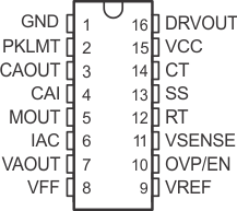
5 Pin Configuration and Functions
D, DW, N, and PW Packages
16 Pins
Top View

Pin Functions
| PIN | I/O | DESCRIPTION | |
|---|---|---|---|
| NAME | NO. | ||
| GND | 1 | – | Ground. All voltages measured with respect to ground. VCC and REF should be bypassed directly to GND with a 0.1-μF or larger ceramic capacitor. |
| PKLMT | 2 | I | PFC peak current limit. The threshold for peak limit is 0 V. Use a resistor divider from the negative side of the current sense resistor to VREF to level shift this signal to a voltage level defined by the value of the sense resistor and the peak current limit. Peak current limit is reached when PKLMT voltage falls below 0 V. |
| CAOUT | 3 | O | Current amplifier output. This is the output of a wide bandwidth operational amplifier that senses line current and commands the PFC pulse-width modulator (PWM) to force the correct duty cycle. Compensation components are placed between CAOUT and MOUT. |
| CAI | 4 | I | Current amplifier noninverting input. Place a resistor between this pin and the GND side of current sense resistor. This input and the inverting input (MOUT) remain functional down to and below GND. |
| MOUT | 5 | I/O | Multiplier output and current amplifier inverting input. The output of the analog multiplier and the inverting input of the current amplifier are connected together at MOUT. As the multiplier output is a current, this is a high-impedance input so the amplifier can be configured as a differential amplifier. This configuration improves noise immunity and allows for the leading-edge modulation operation. The multiplier output current is limited to (2 × IIAC). The multiplier output current is given by the equation: Equation 1.
 where
|
| IAC | 6 | I | Current proportional to input voltage. This input to the analog multiplier is a current proportional to instantaneous line voltage. The multiplier is tailored for very low distortion from this current input (IIAC) to multiplier output. The recommended maximum IIAC is 500 μA. |
| VAOUT | 7 | O | Voltage amplifier output. This is the output of the operational amplifier that regulates output voltage. The voltage amplifier output is internally limited to approximately 5.5 V to prevent overshoot. |
| VFF | 8 | I | Feed-forward voltage. The RMS voltage signal generated at this pin by mirroring 1/2 of the IIAC into a single pole external filter. At low line, the VFF voltage should be 1.4 V. |
| VREF | 9 | O | Voltage reference output. VREF is the output of an accurate 7.5-V voltage reference. This output is capable of delivering 20 mA to peripheral circuitry, and is internally short-circuit current-limited. VREF is disabled and remains at 0 V when VVCC is below the UVLO threshold. Bypass VREF to GND with a 0.1-μF or larger ceramic capacitor for best stability. Refer to Figure 1 and Figure 2 for VREF line and load regulation characteristics. |
| OVP/EN | 10 | I | Over-voltage/enable. A window comparator input that disables the output driver if the boost output voltage is a programmed level above the nominal ,or disables both the PFC output driver and resets SS if pulled below 1.9 V (typ). |
| VSENSE | 11 | I | Voltage amplifier inverting input. This is normally connected to a compensation network and to the boost converter output through a divider network. |
| RT | 12 | I | Oscillator charging current. A resistor from RT to GND is used to program oscillator charging current. A resistor between 10 kΩ and 100 kΩ is recommended. Nominal voltage on this pin is 3 V. |
| SS | 13 | I | Soft-start. VSS is discharged for VVCC low conditions. When enabled, SS charges an external capacitor with a current source. This voltage is used as the voltage error signal during start-up, enabling the PWM duty cycle to increase slowly. In the event of a VVCC dropout, the OVP/EN is forced below 1.9 V (typ), SS quickly discharges to disable the PWM. Note: In an open-loop test circuit, grounding the SS pin does not ensure 0% duty cycle. See the Application and Implementation for details. |
| CT | 14 | I |
Oscillator timing capacitor. A capacitor from CT to GND sets the PWM oscillator frequency according to: Equation 2. f ≈ 0.6/(RT × CT)
The lead from the oscillator timing capacitor to GND should be as short and direct as possible. |
| VCC | 15 | I | Positive supply voltage. Connect to a stable source of at least 20 mA between 10 V and 17 V for normal operation. Bypass VCC directly to GND to absorb supply current spikes required to charge external MOSFET gate capacitances. To prevent inadequate gate drive signals, the output devices are inhibited unless VVCC exceeds the upper undervoltage lockout voltage threshold and remains above the lower threshold. |
| DRVOUT | 16 | O | Gate drive. The output drive for the boost switch is a totem-pole MOSFET gate driver on DRVOUT. Use a series gate resistor to prevent interaction between the gate impedance and the output driver that might cause the DRVOUT to overshoot excessively. See Figure 6 to determine minimum required gate resister value. Some overshoot of the DRVOUT output is always expected when driving a capacitive load. |