JAJS121G September   2003  – April 2017 UCC28220 , UCC28221

PRODUCTION DATA.  

  1. 特長
  2. アプリケーション
  3. 概要
  4. 改訂履歴
  5. Device Comparison Table
  6. Pin Configuration and Functions
  7. Specifications
    1. 7.1 Absolute Maximum Ratings
    2. 7.2 ESD Ratings
    3. 7.3 Recommended Operating Conditions
    4. 7.4 Thermal Information
    5. 7.5 Electrical Characteristics
    6. 7.6 Typical Characteristics
  8. Detailed Description
    1. 8.1 Overview
    2. 8.2 Functional Block Diagram
    3. 8.3 Feature Description
      1. 8.3.1 VDD
      2. 8.3.2 Reference
      3. 8.3.3 Oscillator Operation and Maximum Duty Cycle Setpoint
      4. 8.3.4 Soft Start
      5. 8.3.5 Current Sense
      6. 8.3.6 Output Drivers
    4. 8.4 Device Functional Modes
      1. 8.4.1 Line Overvoltage and Undervoltage
      2. 8.4.2 Start-Up JFET Section
      3. 8.4.3 Slope Compensation
  9. Application and Implementation
    1. 9.1 Application Information
    2. 9.2 Typical Application
      1. 9.2.1 Design Requirements
      2. 9.2.2 Detailed Design Procedure
        1. 9.2.2.1 Overvoltage Protection and Undervoltage Lockout
        2. 9.2.2.2 Peak Current Limit
        3. 9.2.2.3 Current Sense Transformer Reset Resistor (T1 and T2)
        4. 9.2.2.4 Oscillator and Maximum Duty Cycle Clamp
      3. 9.2.3 Application Curves
  10. 10Power Supply Recommendations
  11. 11Layout
    1. 11.1 Layout Guidelines
    2. 11.2 Layout Example
  12. 12デバイスおよびドキュメントのサポート
    1. 12.1 ドキュメントのサポート
      1. 12.1.1 関連資料
    2. 12.2 関連リンク
    3. 12.3 ドキュメントの更新通知を受け取る方法
    4. 12.4 コミュニティ・リソース
    5. 12.5 商標
    6. 12.6 静電気放電に関する注意事項
    7. 12.7 Glossary
  13. 13メカニカル、パッケージ、および注文情報

パッケージ・オプション

デバイスごとのパッケージ図は、PDF版データシートをご参照ください。

メカニカル・データ(パッケージ|ピン)
  • D|16
  • PW|20
サーマルパッド・メカニカル・データ
発注情報

Layout

Layout Guidelines

  1. TI recommends placing a 1-µF ceramic decoupling capacitor as close as possible between the VDD terminal and GND, tracked directly to both terminals.
  2. TI recommends placing a small, external filter capacitor on the CS1 and CS2 terminal. Track the filter capacitor as directly as possible from the CS to GND terminal.
  3. Reduce the total surface area of traces on the CS net to a minimum.
  4. Connect decoupling and noise filter capacitors, as well as sensing resistors directly to the GND terminal in a star-point fashion, ensuring that the current-carrying power tracks (such as the gate drive return) are track separately to avoid noise and ground-drops that could affect the analogue signal integrity.

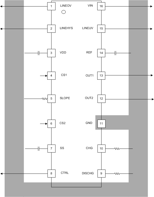
Layout Example

UCC28220 UCC28221 layout.gif Figure 24. UCC28221 Layout