-
UCC28610 Green-Mode Flyback Controller
- 1 Features
- 2 Applications
- 3 Description
- 4 Revision History
- 5 Pin Configuration and Functions
- 6 Specifications
- 7 Detailed Description
- 8 Application and Implementation
- 9 Power Supply Recommendations
- 10Layout
- 11Device and Documentation Support
- 12Mechanical, Packaging, and Orderable Information
- IMPORTANT NOTICE
UCC28610 Green-Mode Flyback Controller
1 Features
- Cascoded Configuration Allows Fully Integrated Current Control Without External Sense Resistor
- Fast Start Up With Low Standby Power Achieved by Cascode Configuration
- Frequency and Peak Current Modulation for Optimum Efficiency Over Entire Operating Range
- Green-Mode (GM) Burst Switching Packets Improve No-Load Efficiency
- Advanced Overcurrent Protection Limits RMS Input and Output Currents
- Thermal Shutdown
- Timed Overload With Retry or Latch-Off Response
- Programmable Opto-Less Output Overvoltage Protection
- Fast Latched Fault Recovery
- 8-Pin SOIC Package and 8-Pin PDIP Lead-Free Packages
2 Applications
- Universal Input AC and DC Adapters, 12 to 65 W
- High Efficiency Housekeeping and Auxillary Power Supplies
- Offline Battery Chargers
- Consumer Electronics (DVD Players, Set-Top Boxes, DTV, Gaming, Printers)
3 Description
The UCC28610 brings a new level of performance and reliability to the AC and DC consumer power supply solution.
A PWM modulation algorithm varies both the switching frequency and primary current while maintaining discontinuous or transition mode operation over the entire operating range. Combined with a cascoded architecture, these innovations result in efficiency, reliability, and system cost improvements over a conventional flyback architecture.
The UCC28610 offers a predictable maximum power threshold and a timed response to an overload, allowing safe handling of surge power requirements. Overload fault response is user-programmed for retry or latch-off mode. Additional protection features include output overvoltage detection, programmable maximum on-time, and thermal shutdown.
Device Information(1)
| PART NUMBER | PACKAGE | BODY SIZE (NOM) |
|---|---|---|
| UCC28610 | SOIC (8) | 4.90 mm x 3.91 mm |
| PDIP (8) | 9.81 mm x 6.35 mm |
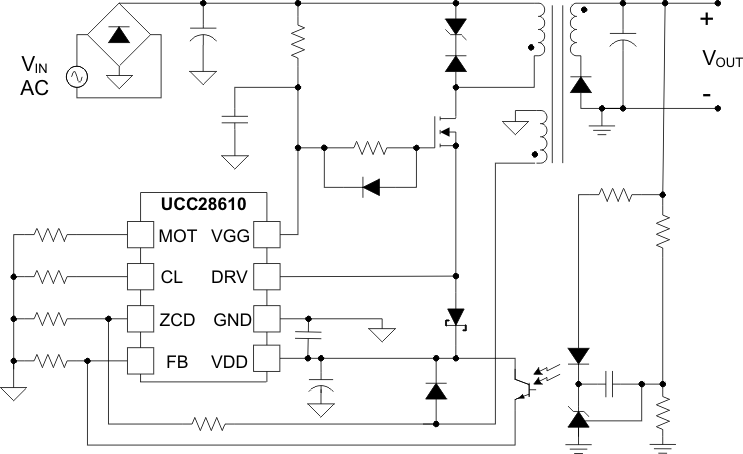
Simplified Application Schematic

4 Revision History
Changes from F Revision (November 2014) to G Revision
- Added Pin Configuration and Functions section, ESD Rating table, Feature Description section, Device Functional Modes, Application and Implementation section, Power Supply Recommendations section, Layout section, Device and Documentation Support section, and Mechanical, Packaging, and Orderable Information section Go
Changes from E Revision (September 2012) to F Revision
- Changed updated typical application drawing on first page.Go
- Added Thermal Information Section.Go
- Changed ESD Rating, Human Body Model from 2000 V to 1500 V.Go
- Changed Electrical Characteristics FB = 0 V to IFB = 10 µA.Go
- Changed Voltage of CL pin max value from 1.05 V to 1.10 V.Go
- Changed IFB range for Green Mode (GM) modulation min value from 50 µA to 45 µA.Go
- Changed ZCD low clamp voltage min value from -200 mV to -220 mV.Go
- Changed Figure 1.Go
- Changed Symplified Block Diagram Go
- Changed Figure 20.Go
- Changed High Frequency Ringing Solutions, (a) ferrite chip, (b) CDRV and (c) RG-OFF drawing.Go
- Changed Basic Flyback Converter and Waveforms at Peak Load and Minimum VBULK Voltage drawing.Go
- Changed Start-Up Currents for the Cascode Architecture drawing.Go
- Changed Feedback Function text.Go
- Changed FB Details drawing.Go
- Changed Modulation Control Blocks drawing.Go
- Changed Control Diagram with Operating Modes drawing.Go
- Changed Recommended Operating Conditions Application drawing.Go
- Changed Basic Flyback Converter and Waveforms at Peak Load and Minimum VBULK Voltage drawing.Go
- Changed Feedback Function text.Go
- Changed FB Details drawing.Go
Changes from D Revision (January 2011) to E Revision
- Changed Symplified Block Diagram Go
Changes from C Revision (January 2009) to D Revision
- Deleted Equation 7 Go
- Deleted Equation 7 Go
5 Pin Configuration and Functions


Pin Functions
| PIN | I/O | DESCRIPTION | ||
|---|---|---|---|---|
| NAME | NO. | |||
| CL | 3 | I | (Current Limit) This pin programs the peak primary inductor current that is reached each switching cycle. Program with a resistor between CL and GND. | |
| DRV | 6 | O | (DRiVe) This pin drives the source of an external high voltage power MOSFET. The DRV pin carries the full primary current of the converter. Connect a Schottky diode between DRV and VDD to provide initial bias at start up. | |
| FB | 1 | I | (FeedBack) The FB current, IFB, commands the operating mode of the UCC28610. The FB voltage is always 0.7 V. This pin only detects current. | |
| GND | 7 | — | (GrouND) This pin is the current return terminal for both the analog and power signals in the UCC28610. This terminal carries the full primary current of the converter. Separate the return path of the bulk capacitor from the return path of FB, ZCD, MOT, and CL. | |
| MOT | 4 | I | (Maximum On Time) This pin has three functions:
Functions 1 and 2 are programmed with a resistor between MOT and GND. |
|
| VDD | 8 | — | This is the bias supply pin for the UCC28610. It can be derived from an external source or an auxiliary winding. This pin must be decoupled with a 0.1-μF ceramic capacitor placed between VDD and GND, as close to the device as possible. | |
| VGG | 5 | — | This pin provides a DC voltage for the gate of the external high voltage MOSFET. This pin must be decoupled with a 0.1-μF ceramic capacitor placed between VGG and GND, as close to the device as possible. This pin also initiates start-up bias through a large value resistor that is connected to the input bulk voltage. | |
| ZCD | 2 | I | (Zero Current Detection) This pin has two functions:
|
|