JAJSDB5 June 2017 UCC28730-Q1
PRODUCTION DATA.
- 1 特長
- 2 アプリケーション
- 3 概要
- 4 改訂履歴
- 5 Pin Configuration and Functions
- 6 Specifications
-
7 Detailed Description
- 7.1 Overview
- 7.2 Functional Block Diagram
- 7.3 Feature Description
- 7.4 Device Functional Modes
-
8 Application and Implementation
- 8.1 Application Information
- 8.2
Typical Application
- 8.2.1 Design Requirements
- 8.2.2
Detailed Design Procedure
- 8.2.2.1 Stand-By Power Estimate
- 8.2.2.2 Input Bulk Capacitance and Minimum Bulk Voltage
- 8.2.2.3 Transformer Turns Ratio, Inductance, Primary-Peak Current
- 8.2.2.4 Transformer Parameter Verification
- 8.2.2.5 Output Capacitance
- 8.2.2.6 VDD Capacitance, CVDD
- 8.2.2.7 VS Resistor Divider, Line Compensation, and Cable Compensation
- 8.2.2.8 VS Wake-Up Detection
- 8.2.3 Application Curves
- 8.3 Do's and Don'ts
- 9 Power Supply Recommendations
- 10Layout
- 11デバイスおよびドキュメントのサポート
- 12メカニカル、パッケージ、および注文情報
10 Layout
10.1 Layout Guidelines
In order to increase the reliability and feasibility of the project it is recommended to adhere to the following guidelines for PCB layout.
- Minimize stray capacitance on the VS node. Place the voltage sense resistors (RS1 and RS2 in Figure 24 through Figure 27) close to the VS pin.
- TI recommends to connect the HV input to a non-switching source of high voltage, not to the MOSFET drain, to avoid injecting high-frequency capacitive current pulses into the device.
- Arrange the components to minimize the loop areas of the switching currents as much as possible. These areas include such loops as the transformer primary winding current loop, the MOSFET gate-drive loop, the primary snubber loop, the auxiliary winding loop and the secondary output current loop.
10.2 Layout Example
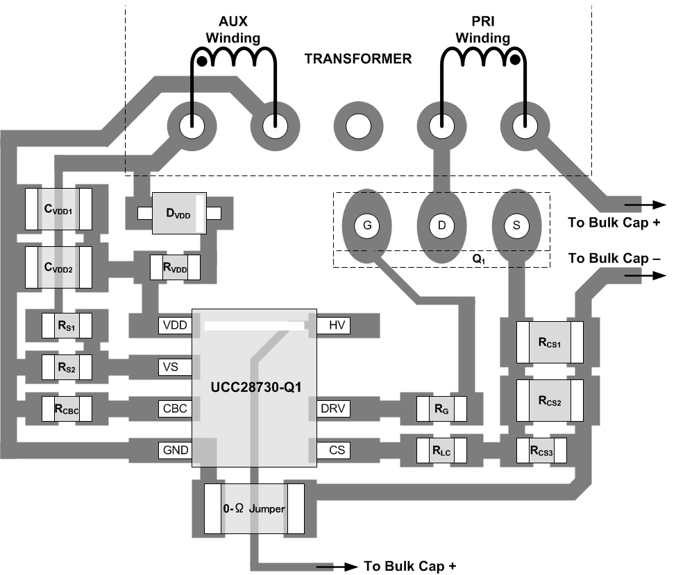
The partial layout example of Figure 28 demonstrates an effective component and track arrangement for low-noise operation on a single-layer printed circuit board. Actual board layout must conform to the constraints on a specific design, so many variations are possible.
 Figure 28. UCC28730-Q1 Partial Layout Example