JAJSHT2C august 2019 – december 2020 UCC28740-Q1
PRODUCTION DATA
- 1
- 1 特長
- 2 アプリケーション
- 3 概要
- 4 Revision History
- 5 Revision History
- 6 Revision History
- 7 Pin Configuration and Functions
- 8 Specifications
- 9 Detailed Description
-
10Application and Implementation
- 10.1 Application Information
- 10.2 High Voltage Applications
- 10.3
Typical Application
- 10.3.1 Design Requirements
- 10.3.2
Detailed Design Procedure
- 10.3.2.1 Custom Design With WEBENCH® Tools
- 10.3.2.2 Standby Power Estimate and No-Load Switching Frequency
- 10.3.2.3 Input Bulk Capacitance and Minimum Bulk Voltage
- 10.3.2.4 38
- 10.3.2.5 Transformer Turns-Ratio, Inductance, Primary Peak Current
- 10.3.2.6 Transformer Parameter Verification
- 10.3.2.7 VS Resistor Divider, Line Compensation
- 10.3.2.8 Output Capacitance
- 10.3.2.9 VDD Capacitance, CVDD
- 10.3.2.10 Feedback Network Biasing
- 10.3.3 Application Curves
- 11Power Supply Recommendations
- 12Layout
-
13Device and Documentation Support
- 13.1
Device Support
- 13.1.1 Development Support
- 13.1.2
Device Nomenclature
- 13.1.2.1 Capacitance Terms in Farads
- 13.1.2.2 Duty Cycle Terms
- 13.1.2.3 Frequency Terms in Hertz
- 13.1.2.4 Current Terms in Amperes
- 13.1.2.5 Current and Voltage Scaling Terms
- 13.1.2.6 Transformer Terms
- 13.1.2.7 Power Terms in Watts
- 13.1.2.8 Resistance Terms in Ohms
- 13.1.2.9 Timing Terms in Seconds
- 13.1.2.10 Voltage Terms in Volts
- 13.1.2.11 AC Voltage Terms in VRMS
- 13.1.2.12 Efficiency Terms
- 13.2 Documentation Support
- 13.3 Receiving Notification of Documentation Updates
- 13.4 Community Resources
- 13.5 Trademarks
- 13.1
Device Support
- Mechanical, Packaging, and Orderable Information
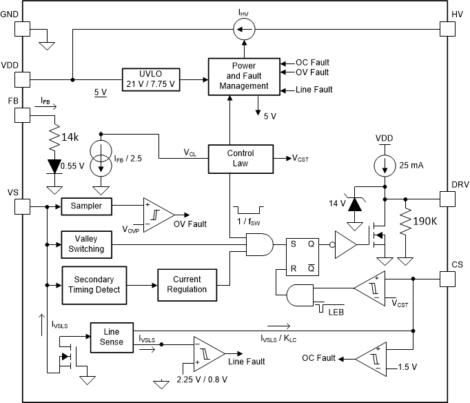
9.2 Functional Block Diagram
