JAJSOG3 December   2023 UCC28750

PRODUCTION DATA  

  1.   1
  2. 特長
  3. アプリケーション
  4. 概要
  5. Device Comparison
  6. Pin Configuration and Functions
  7. Specifications
    1. 6.1 Absolute Maximum Ratings
    2. 6.2 ESD Ratings
    3. 6.3 Recommended Operating Conditions
    4. 6.4 Thermal Information
    5. 6.5 Electrical Characteristics
    6. 6.6 Switching Characteristics
    7. 6.7 Timing Requirements
    8. 6.8 Typical Characteristics
  8. Detailed Description
    1. 7.1 Overview
    2. 7.2 Functional Block Diagram
    3. 7.3 Detailed Pin Descriptions
      1. 7.3.1 VDD - Input Bias
      2. 7.3.2 DRV - Gate Drive Out
      3. 7.3.3 CS - Current Sensing
      4. 7.3.4 FB - Feedback
      5. 7.3.5 FLT - Fault
      6. 7.3.6 GND - Ground Return
    4. 7.4 Feature Description
      1. 7.4.1 Soft Start
      2. 7.4.2 Control Law
      3. 7.4.3 Frequency Dithering
      4. 7.4.4 Fault Protections
        1. 7.4.4.1 VDD Overvoltage and Undervoltage Lockout
        2. 7.4.4.2 Internal Overtemperature Protection
        3. 7.4.4.3 Output Overpower Protection
        4. 7.4.4.4 Output Short-Circuit Protection
        5. 7.4.4.5 FLT Pin Protections
      5. 7.4.5 Slope Compensation
    5. 7.5 Device Functional Modes
      1. 7.5.1 Off
      2. 7.5.2 Startup
      3. 7.5.3 On
      4. 7.5.4 Fault
      5. 7.5.5 Disabled
  9. Application and Implementation
    1. 8.1 Application Information
    2. 8.2 Typical Application
      1. 8.2.1 Application
      2. 8.2.2 Design Requirements
      3. 8.2.3 Detailed Design Procedure
        1. 8.2.3.1 Input Bulk Capacitance with Minimum Bulk Voltage
        2. 8.2.3.2 Transformer Turns Ratio and Inductance
        3. 8.2.3.3 Current Sense and Slope Compensation Network
        4. 8.2.3.4 Output Capacitors
        5. 8.2.3.5 VDD Capacitance, CVDD
      4. 8.2.4 Application Performance Plots
        1. 8.2.4.1 Startup
        2. 8.2.4.2 Load Transients
        3. 8.2.4.3 Q1 Drain Voltage Evaluation
      5. 8.2.5 What to Do and What Not to Do
    3. 8.3 Power Supply Recommendations
    4. 8.4 Layout
      1. 8.4.1 Layout Guidelines
      2. 8.4.2 Layout Example
  10. Device and Documentation Support
    1. 9.1 Documentation Support
      1. 9.1.1 Related Documentation
    2. 9.2 ドキュメントの更新通知を受け取る方法
    3. 9.3 サポート・リソース
    4. 9.4 Trademarks
    5. 9.5 静電気放電に関する注意事項
    6. 9.6 用語集
  11. 10Revision History
  12. 11Mechanical, Packaging, and Orderable Information

パッケージ・オプション

メカニカル・データ(パッケージ|ピン)
サーマルパッド・メカニカル・データ
発注情報

Startup

CH1 =VBULK , CH2 = VCC, CH3 = VGATE, CH4 = VOUT
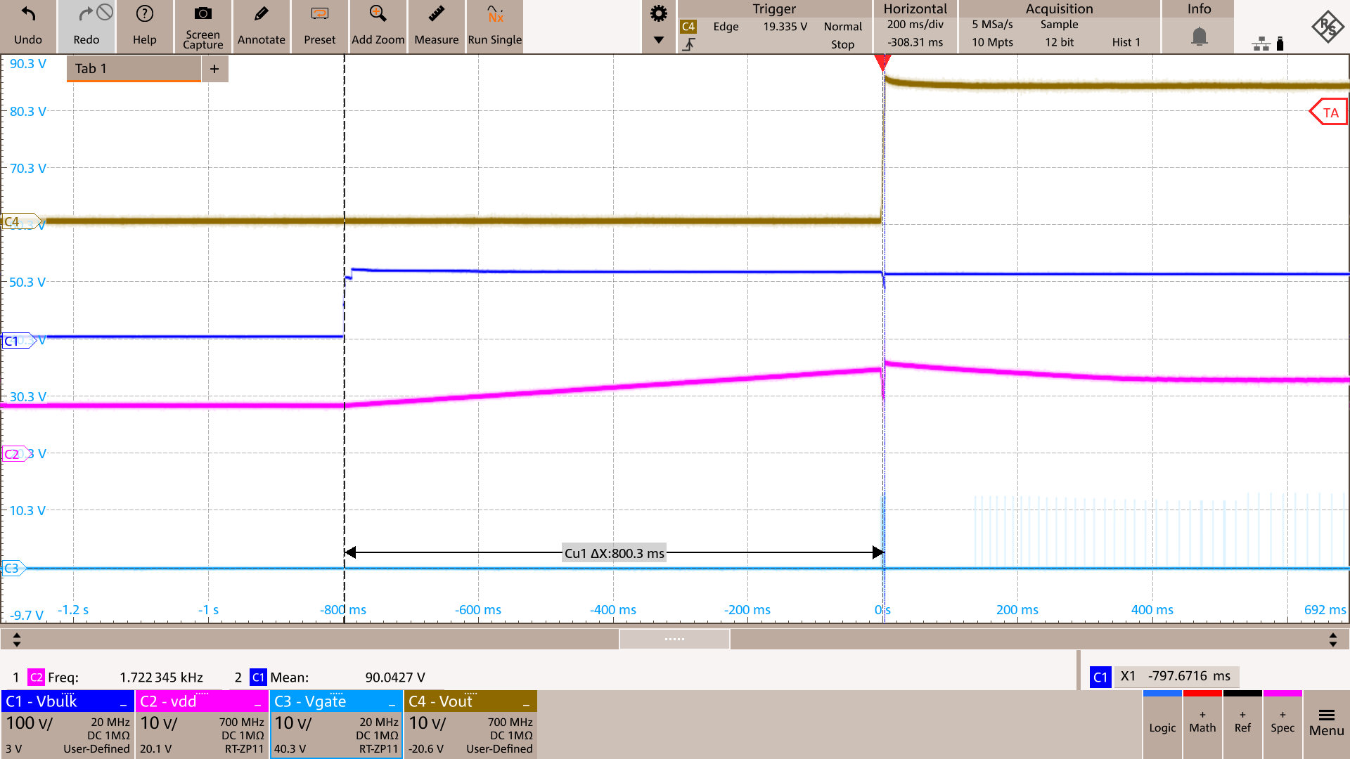
GUID-20231107-SS0I-D3K2-PSMG-D32NNKS3X9QZ-low.pngFigure 8-4 Start-Up Waveforms at 85Vac and No Load
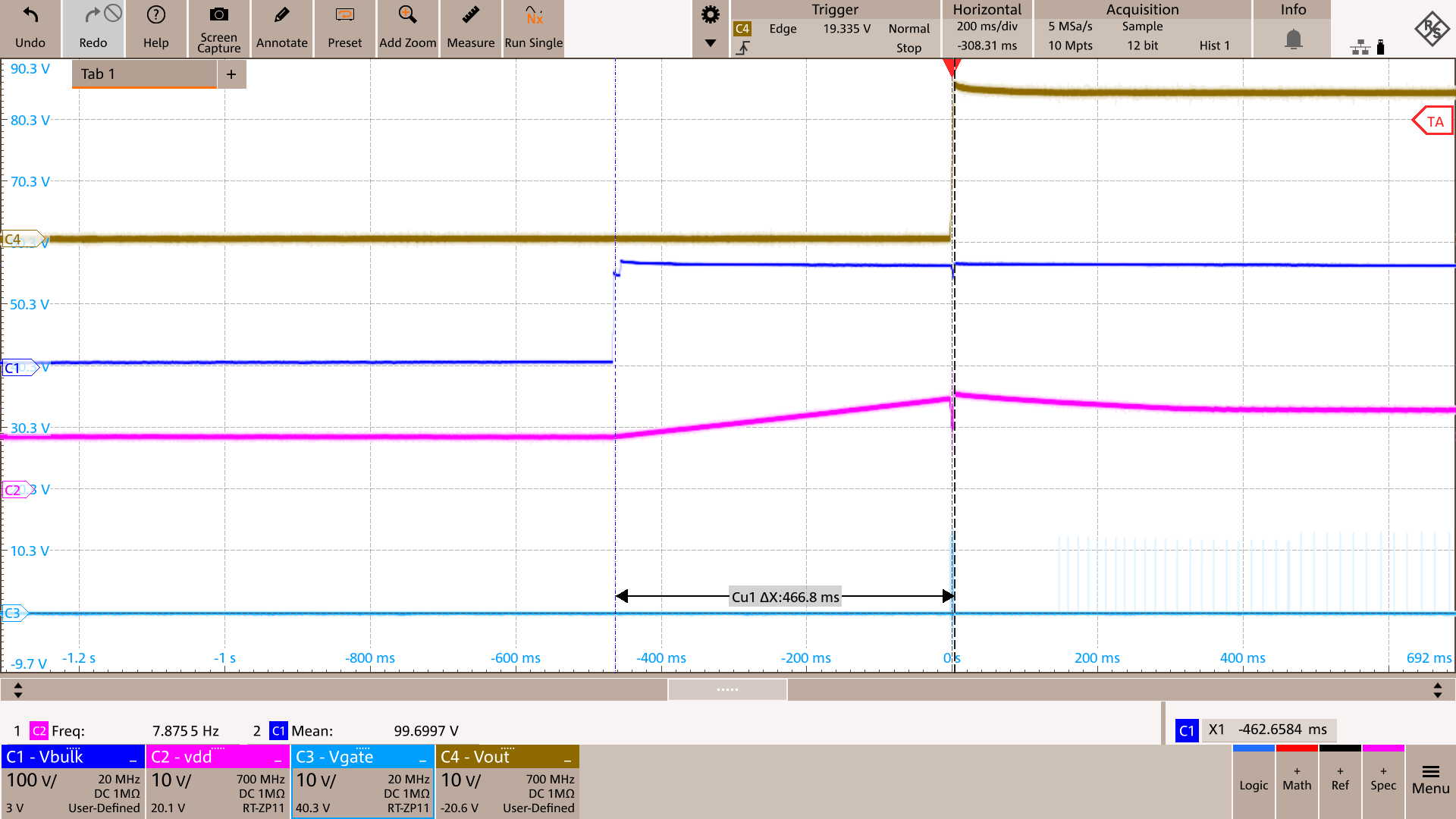
GUID-20231107-SS0I-TLNN-LJ9K-FV0PX0RFNVW3-low.pngFigure 8-6 Start-Up Waveforms at 115Vac and No Load
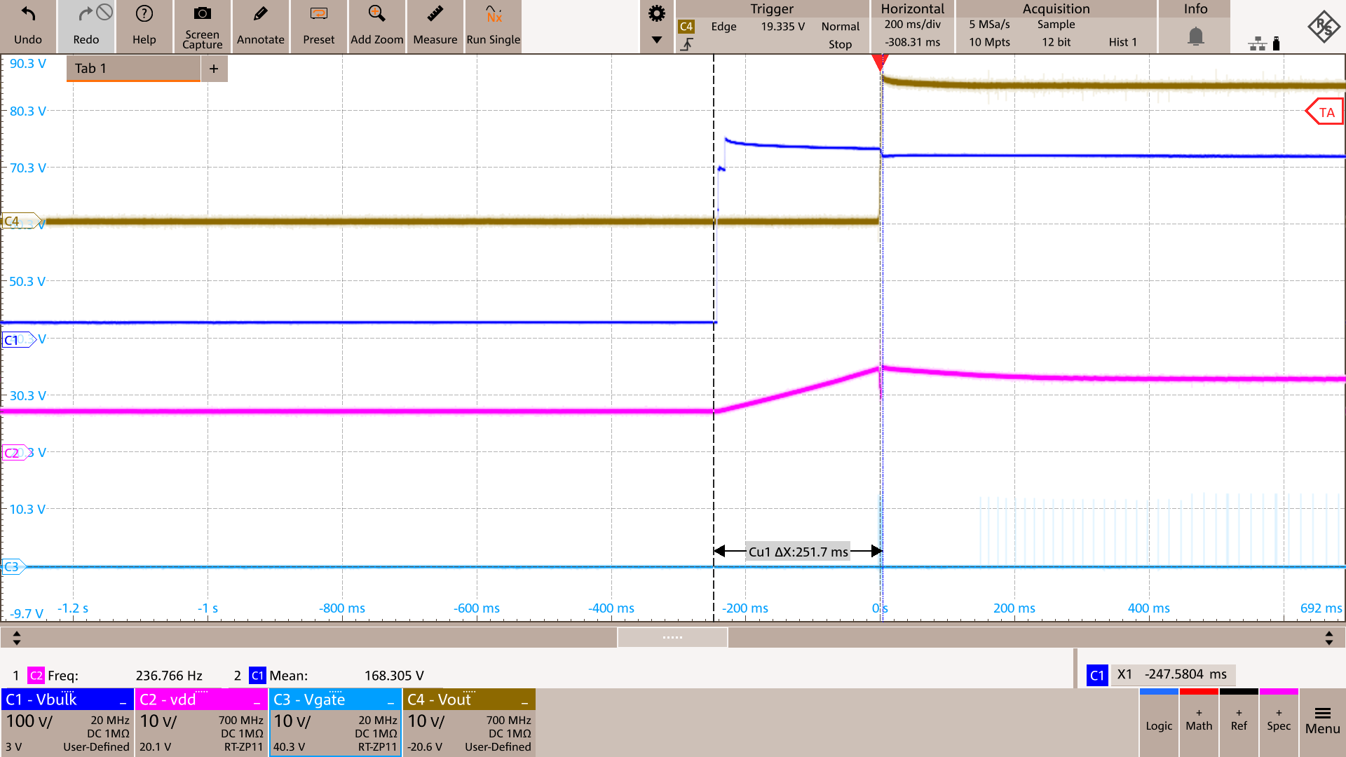
GUID-20231107-SS0I-MS4Z-JLWX-S3DBHJSWG7BV-low.pngFigure 8-8 Start-Up Waveforms at 230Vac and No Load
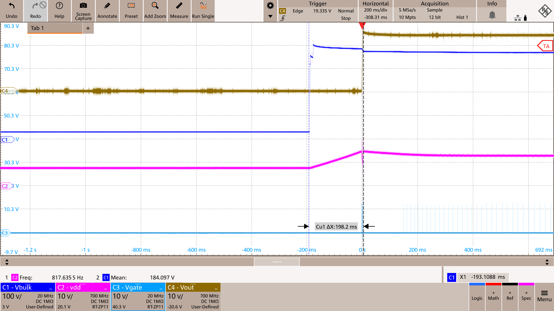
GUID-20231107-SS0I-LZLR-BQ2T-K1NTSZ5TT0JQ-low.pngFigure 8-10 Start-Up Waveforms at 265Vac and No Load
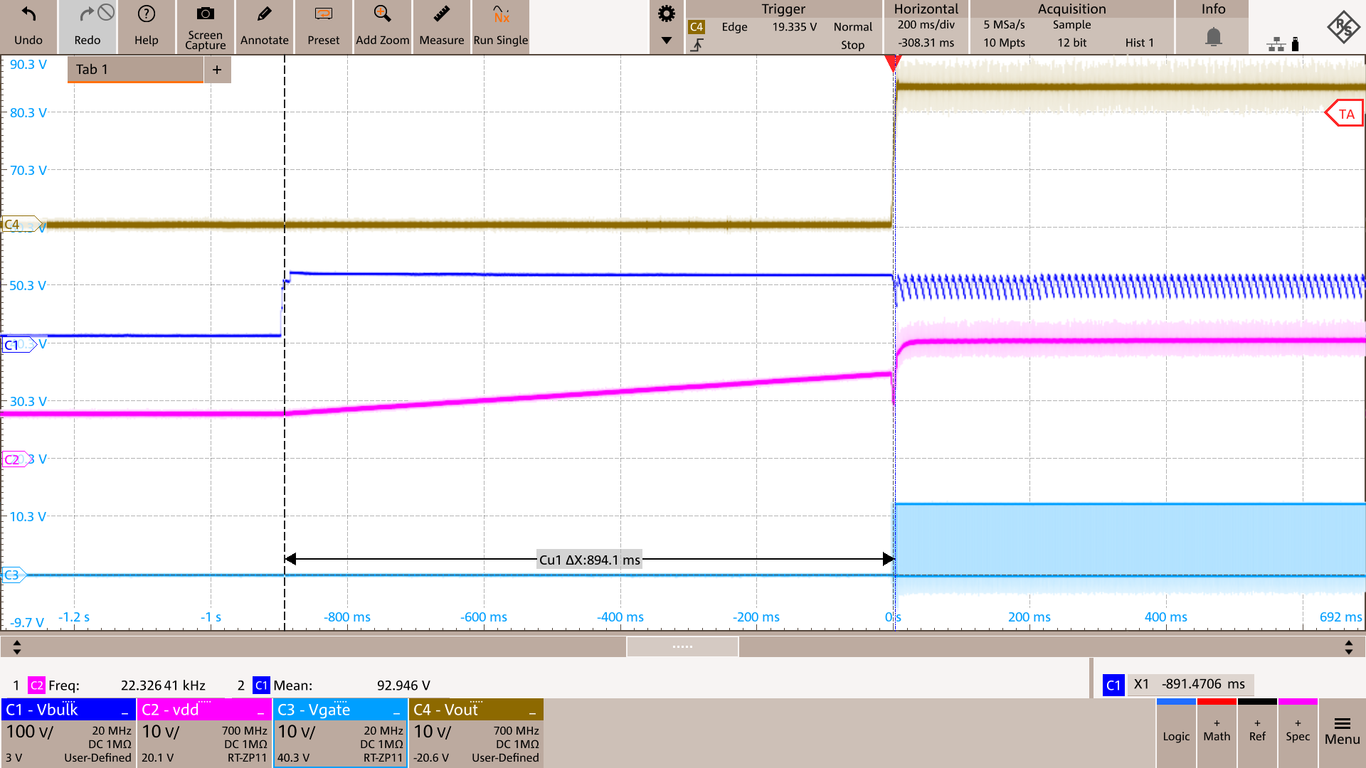
GUID-20231107-SS0I-HDCB-6V08-K1XCJVPMSPPC-low.pngFigure 8-5 Start-Up Waveforms at 85Vac and Full Load
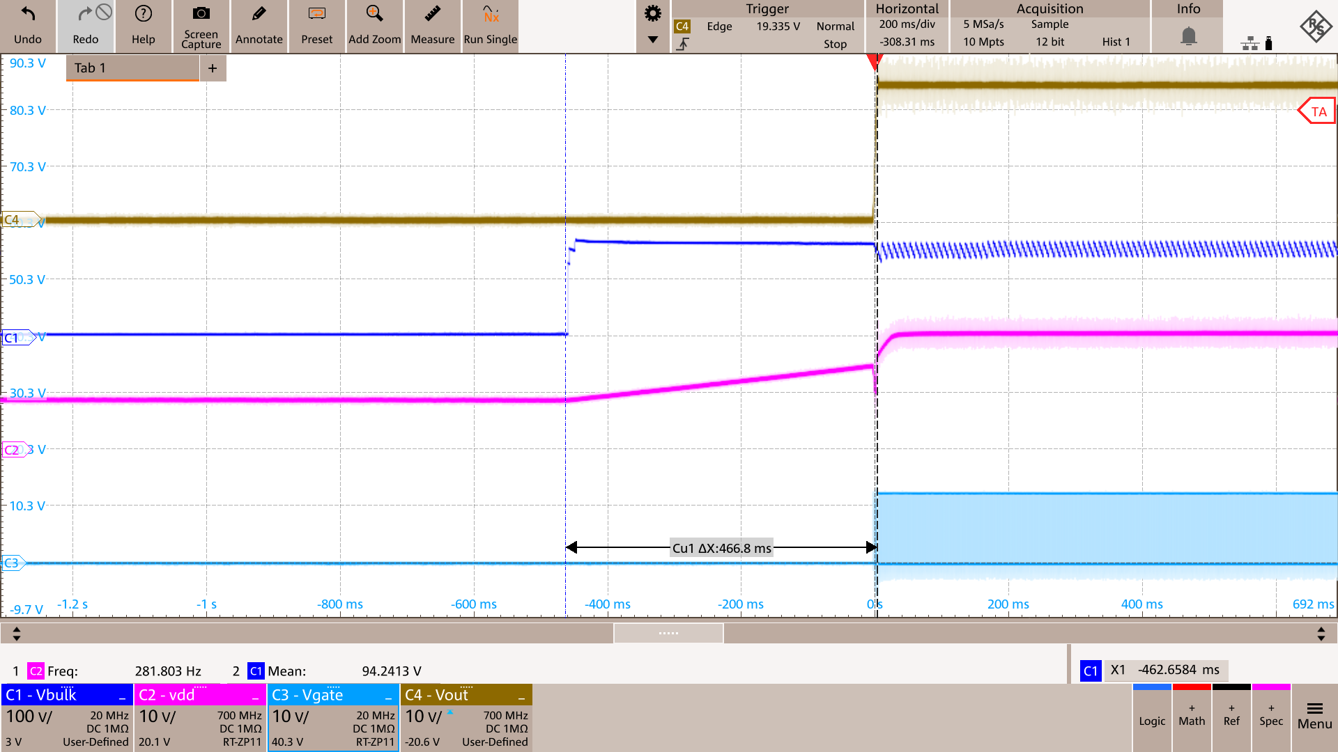
GUID-20231107-SS0I-FVTG-LKJ6-KV59P5QB6ZHC-low.pngFigure 8-7 Start-Up Waveforms at 115Vac and Full Load
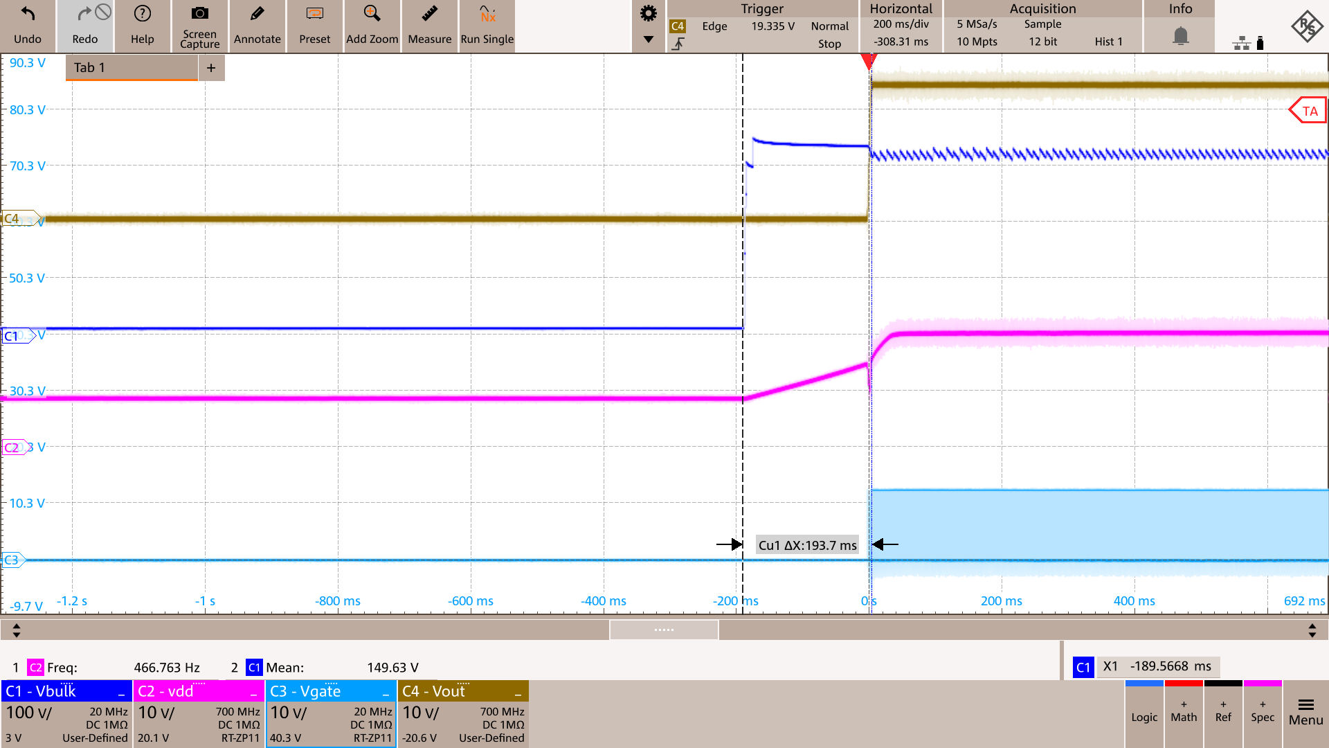
GUID-20231107-SS0I-T15V-BHN6-KLBBDP9XRT9C-low.pngFigure 8-9 Start-Up Waveforms at 230Vac and Full Load
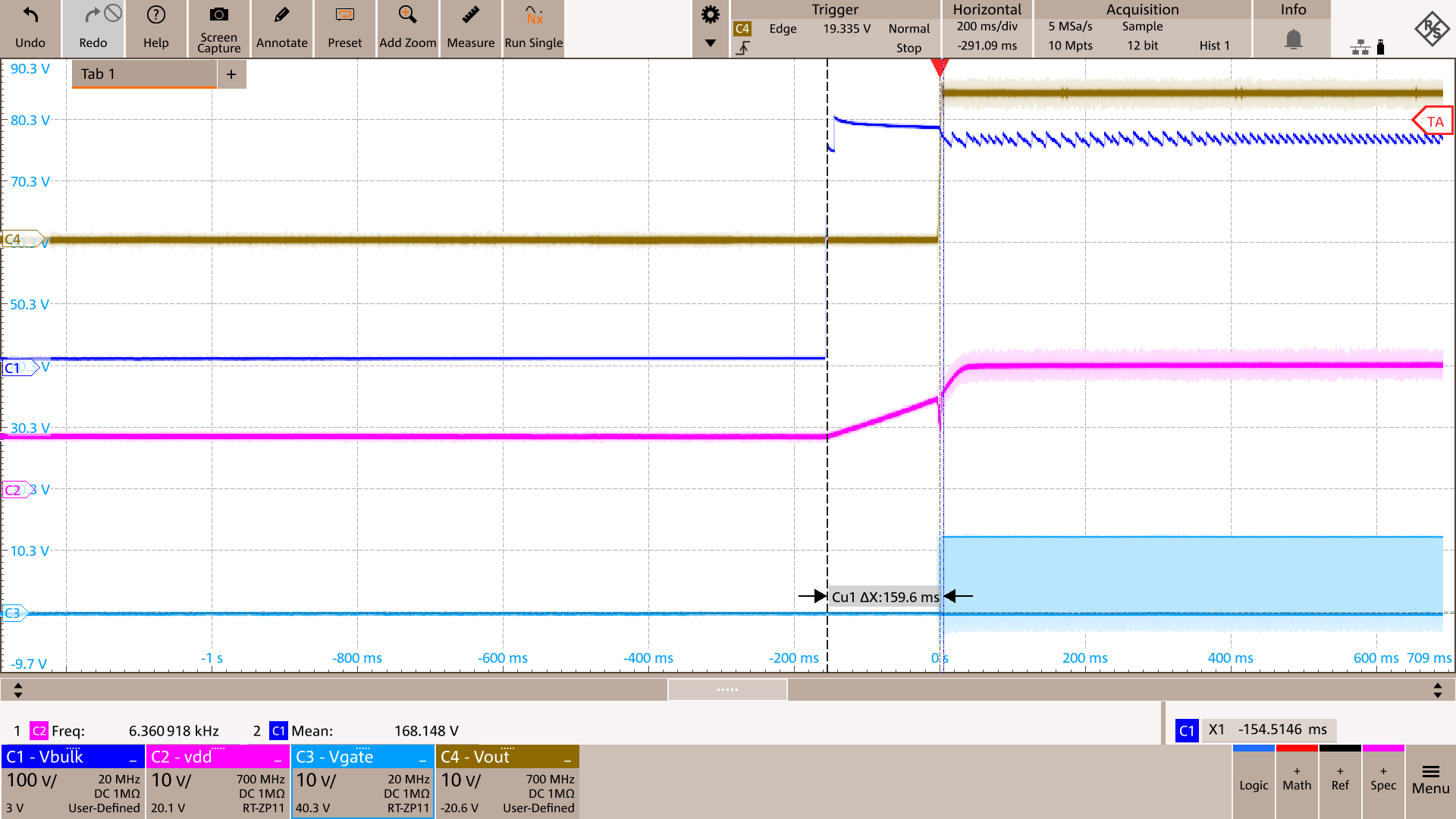
GUID-20231107-SS0I-MSZD-DLT5-3MWFCDTLKMTD-low.pngFigure 8-11 Start-Up Waveforms at 265Vac and Full Load