JAJSLC6 November 2021 UCC28781-Q1
PRODUCTION DATA
- 1 特長
- 2 アプリケーション
- 3 概要
- 4 Revision History
- 5 Pin Configuration and Functions
- 6 Specifications
-
7 Detailed Description
- 7.1 Overview
- 7.2 Functional Block Diagram
- 7.3
Detailed Pin Description
- 7.3.1 BUR Pin (Programmable Burst Mode)
- 7.3.2 FB Pin (Feedback Pin)
- 7.3.3 REF Pin (Internal 5-V Bias)
- 7.3.4 VDD Pin (Device Bias Supply)
- 7.3.5 P13 and SWS Pins
- 7.3.6 S13 Pin
- 7.3.7 IPC Pin (Intelligent Power Control Pin)
- 7.3.8 RUN Pin (Driver and Bias Source for Isolator)
- 7.3.9 PWMH and AGND Pins
- 7.3.10 PWML and PGND Pins
- 7.3.11 SET Pin
- 7.3.12 RTZ Pin (Sets Delay for Transition Time to Zero)
- 7.3.13 RDM Pin (Sets Synthesized Demagnetization Time for ZVS Tuning)
- 7.3.14 XCD Pin
- 7.3.15 CS, VS, and FLT Pins
- 7.4
Device Functional Modes
- 7.4.1 Adaptive ZVS Control with Auto-Tuning
- 7.4.2 Dead-Time Optimization
- 7.4.3 EMI Dither and Dither Fading Function
- 7.4.4 Control Law Across Entire Load Range
- 7.4.5 Adaptive Amplitude Modulation (AAM)
- 7.4.6 Adaptive Burst Mode (ABM)
- 7.4.7 Low Power Mode (LPM)
- 7.4.8 First Standby Power Mode (SBP1)
- 7.4.9 Second Standby Power Mode (SBP2)
- 7.4.10 Startup Sequence
- 7.4.11 Survival Mode of VDD (INT_STOP)
- 7.4.12
System Fault Protections
- 7.4.12.1 Brown-In and Brown-Out
- 7.4.12.2 Output Over-Voltage Protection (OVP)
- 7.4.12.3 Input Over Voltage Protection (IOVP)
- 7.4.12.4 Over-Temperature Protection (OTP) on FLT Pin
- 7.4.12.5 Over-Temperature Protection (OTP) on CS Pin
- 7.4.12.6 Programmable Over-Power Protection (OPP)
- 7.4.12.7 Peak Power Limit (PPL)
- 7.4.12.8 Output Short-Circuit Protection (SCP)
- 7.4.12.9 Over-Current Protection (OCP)
- 7.4.12.10 External Shutdown
- 7.4.12.11 Internal Thermal Shutdown
- 7.4.13 Pin Open/Short Protections
-
8 Application and Implementation
- 8.1 Application Information
- 8.2
Typical Application Circuit
- 8.2.1 Design Requirements for a 60-W, 15-V ZVSF Bias Supply Application with a DC Input
- 8.2.2 Detailed Design Procedure
- 8.2.3 Application Curves
- 9 Power Supply Recommendations
- 10Layout
- 11Device and Documentation Support
- 12Mechanical, Packaging, and Orderable Information
7.3.7 IPC Pin (Intelligent Power Control Pin)
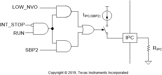
Under certain conditions, the IPC pin provides a 50-µA current from an internal source (IIPC(SBP2)) which is controlled by logic as shown in #X2692. The voltage on the VS pin is sampled during the demagnetization time to obtain an indication of the reflected output voltage (NVO). When the VS-pin voltage is lower than the 2.4-V lower LV mode threshold (VVSLV(LR)), the LOW_NVO logic signal is pulled high, and the current source is enabled during the run state of all normal control modes (SBP1, SBP2, LPM, ABM, and AAM).
When the sampled VS-pin voltage is higher than the 2.5-V upper LV mode threshold (VVSLV(UP)), the LOW_NVO logic signal becomes low. In the LOW_NVO = 0 V case, the 50-µA current source is enabled in the run state of SBP2 mode only.
To minimize stand-by power, the 50-µA source is always disabled during the wait state of any control mode. Additionally, if VVDD falls lower than the 13-V survival-mode threshold, the INT_STOP logic signal is pulled high and the current source is disabled during survival mode operation, irrespective of the VVS level.
 Figure 7-9 Control
Circuit Diagram to the IPC-Pin Current Source
Figure 7-9 Control
Circuit Diagram to the IPC-Pin Current SourceThe multi-function IPC pin can be programmed to obtain one or more of the following benefits:
- Reduction of input power for special light-load and stand-by conditions
- Improvement of light-load efficiency at lower output voltages, such as 5 V and 9 V
- Reduction of burst-mode output ripple at lower output voltages
- Reduction of the over-power limit at lower output voltages
- Power management of a PFC controller, together with the S13 pin
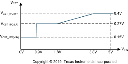
To implement the benefit No. 1, connect a resistor RIPC from IPC pin to AGND pin. The 50-µA current source establishes a voltage (VIPC) across RIPC to program an increase in the CS-pin peak primary current threshold at very light loads. The transfer function between VIPC and the CS threshold (VCST_IPC) in SBP2 mode is illustrated in #X4081.
Proper sizing of RIPC to AGND can further reduce the burst frequency in SBP2 for so-called tiny-load power and for stand-by power.
When VIPC is less than 0.9 V (or IPC is shorted to AGND), VCST_IPC threshold stays at the minimum level of 0.15 V. When VIPC is set between 0.9 V and 1.8 V, VCST_IPC is clamped at 0.27 V. For VIPC between 1.8 V and 3.8 V, there is a linear programmable VCST_IPC range between 0.27 V and 0.4 V. When VIPC is greater than 3.8 V, VCST_IPC remains clamped to 0.4 V. Be aware that high settings of VCST_IPC may, in some cases, introduce higher output ripple in deep light-load condition or provoke audible noise.
 Figure 7-10 IPC Transfer Function to Program the SBP2 Peak Current Threshold
Because the enable status of the IPC current source contains the very useful output voltage information from the LOW_NVO logic state, the IPC pin can be used to further optimize power stage performance over a wide output voltage range. To gain benefits No.2, No. 3, and No. 4 of the IPC function, connect RIPC between the IPC pin and the CS pin, so that the current source can create additional CS-pin offset voltage on ROPP when VVS < 2.4 V. With higher CS offset, the operating range of the VCST signal will be higher than the actual power stage peak current. This forces the controller to operate in AAM mode for a wider actual output load range, and forces the burst-mode threshold down to a lower power level.
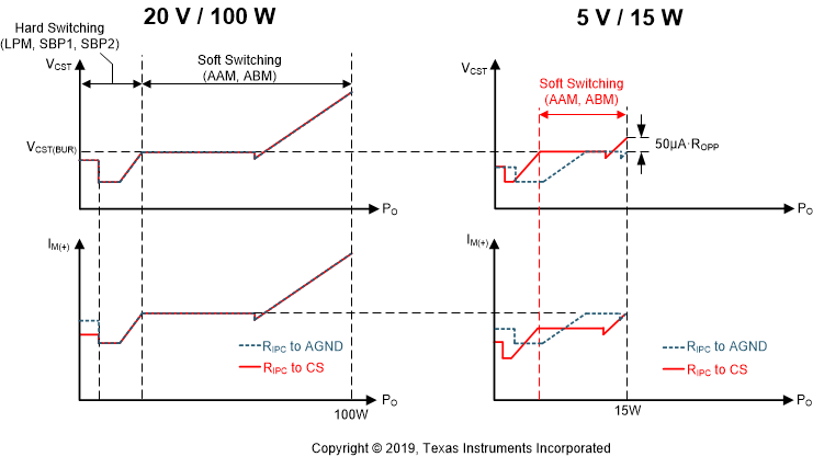
#X5856 shows the side effect of the IPC-to-CS connection if the RIPC setting is the same. Because the controller enables 50 µA in the run state of SBP2, the lower peak magnetizing current of the IPC-to-CS connection makes the SBP2 burst frequency higher and results in weakening the stand-by power improvement. Therefore, a higher RIPC is needed to increase VCST_IPC to compensate the peak current change.
 Figure 7-11 Effect of the CS-pin Offset Voltage from the IPC Pin
For benefit No. 5, the IPC pin can also be used to disable a PFC controller (if used) at all load conditions for lower voltage outputs to further improve the light-load efficiency . As shown in Power Management Function for a GaN Power IC and PFC Controller, the diode DIPC in series with RIPC is placed between IPC and CS pins, and VIPC established at IPC is used to drive a small-signal switch QIPC to disable the PFC controller such as UCC28056.
When VIPC is higher than its threshold voltage, QIPC can pull low the COMP pin voltage of a PFC controller, so its switching is disabled. As a consequence, PFC output voltage drops from the typical 400-V regulation level to the peak value of the AC line. This lowers the bulk voltage, which reduces the ZVS energy, which increases power stage efficiency for low voltage outputs. Furthermore, the power loss of the PFC power stage is out of the efficiency equation. One design example for those components are CS13(ZVSF) = 22 nF, CS13(PFC) = 0.22 µF, CIPC = 10 nF, RIPC = 69.8 kΩ, RIPC2 = 10 MΩ, and RIPC3 = 20 kΩ. Choose QIPC with threshold voltage less than 1.5 V to ensure that VIPC is sufficient to achieve low on-resistance (RDS(on)) even at very low burst frequencies.