JAJSLC6 November 2021 UCC28781-Q1
PRODUCTION DATA
- 1 特長
- 2 アプリケーション
- 3 概要
- 4 Revision History
- 5 Pin Configuration and Functions
- 6 Specifications
-
7 Detailed Description
- 7.1 Overview
- 7.2 Functional Block Diagram
- 7.3
Detailed Pin Description
- 7.3.1 BUR Pin (Programmable Burst Mode)
- 7.3.2 FB Pin (Feedback Pin)
- 7.3.3 REF Pin (Internal 5-V Bias)
- 7.3.4 VDD Pin (Device Bias Supply)
- 7.3.5 P13 and SWS Pins
- 7.3.6 S13 Pin
- 7.3.7 IPC Pin (Intelligent Power Control Pin)
- 7.3.8 RUN Pin (Driver and Bias Source for Isolator)
- 7.3.9 PWMH and AGND Pins
- 7.3.10 PWML and PGND Pins
- 7.3.11 SET Pin
- 7.3.12 RTZ Pin (Sets Delay for Transition Time to Zero)
- 7.3.13 RDM Pin (Sets Synthesized Demagnetization Time for ZVS Tuning)
- 7.3.14 XCD Pin
- 7.3.15 CS, VS, and FLT Pins
- 7.4
Device Functional Modes
- 7.4.1 Adaptive ZVS Control with Auto-Tuning
- 7.4.2 Dead-Time Optimization
- 7.4.3 EMI Dither and Dither Fading Function
- 7.4.4 Control Law Across Entire Load Range
- 7.4.5 Adaptive Amplitude Modulation (AAM)
- 7.4.6 Adaptive Burst Mode (ABM)
- 7.4.7 Low Power Mode (LPM)
- 7.4.8 First Standby Power Mode (SBP1)
- 7.4.9 Second Standby Power Mode (SBP2)
- 7.4.10 Startup Sequence
- 7.4.11 Survival Mode of VDD (INT_STOP)
- 7.4.12
System Fault Protections
- 7.4.12.1 Brown-In and Brown-Out
- 7.4.12.2 Output Over-Voltage Protection (OVP)
- 7.4.12.3 Input Over Voltage Protection (IOVP)
- 7.4.12.4 Over-Temperature Protection (OTP) on FLT Pin
- 7.4.12.5 Over-Temperature Protection (OTP) on CS Pin
- 7.4.12.6 Programmable Over-Power Protection (OPP)
- 7.4.12.7 Peak Power Limit (PPL)
- 7.4.12.8 Output Short-Circuit Protection (SCP)
- 7.4.12.9 Over-Current Protection (OCP)
- 7.4.12.10 External Shutdown
- 7.4.12.11 Internal Thermal Shutdown
- 7.4.13 Pin Open/Short Protections
-
8 Application and Implementation
- 8.1 Application Information
- 8.2
Typical Application Circuit
- 8.2.1 Design Requirements for a 60-W, 15-V ZVSF Bias Supply Application with a DC Input
- 8.2.2 Detailed Design Procedure
- 8.2.3 Application Curves
- 9 Power Supply Recommendations
- 10Layout
- 11Device and Documentation Support
- 12Mechanical, Packaging, and Orderable Information
7.4.5 Adaptive Amplitude Modulation (AAM)
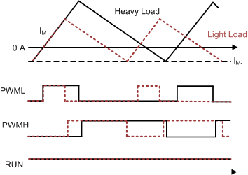
The switching pattern in AAM forces PWML and PWMH to alternate in a complementary fashion with dead-time in between, as shown in #T4924628-31. As the load current reduces, the negative magnetizing current (IM-) stays the same, while the positive magnetizing current (IM+) reduces by the internal peak current loop to regulate the output voltage. IM+ generates a current-feedback signal (VCS) on the CS pin through a current-sense resistor (RCS) in series with QL source and a peak current threshold (VCST) in the current loop controls the peak current variation. Due to the nature of transition-mode (TM) operation, lowering the peak current with lighter load conditions results in higher switching frequency. When the load current increases to an over-power condition (IO(OPP)) where VCST correspondingly reaches an OPP threshold (VCST(OPP)) of the peak current loop, the OPP fault response will be triggered after a 160-ms timeout. The RUN signal stays high in AAM, so the half-bridge driver remains active.
 Figure 7-30 PWM Pattern in AAM