SLUSDV5B October 2019 – April 2020 UCC5304
PRODUCTION DATA.
- 1 Features
- 2 Applications
- 3 Description
- 4 Revision History
- 5 Pin Configuration and Functions
-
6 Specifications
- 6.1 Absolute Maximum Ratings
- 6.2 ESD Ratings
- 6.3 Recommended Operating Conditions
- 6.4 Thermal Information
- 6.5 Power Ratings
- 6.6 Insulation Specifications
- 6.7 Safety-Related Certifications
- 6.8 Safety-Limiting Values
- 6.9 Electrical Characteristics
- 6.10 Switching Characteristics
- 6.11 Typical Characteristics
- 7 Parameter Measurement Information
- 8 Detailed Description
- 9 Application and Implementation
- 10Power Supply Recommendations
- 11Layout
- 12Mechanical, Packaging, and Orderable Information
7.2 Power-up UVLO Delay to OUTPUT
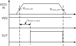
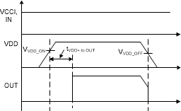
Before the driver is ready to deliver a proper output state, there is a power-up delay from the UVLO rising edge to output and it is defined as tVCCI+ to OUT for VCCI UVLO, which is 40 µs typically, and tVDD+ to OUT for VDD UVLO, which is 22 µs typically. It is recommended to allow proper delay margin after the driver VCCI and VDD bias supplies are ready before applying the PWM signal at the IN pin. Figure 18 and Figure 19 show the power-up UVLO delay timing diagram for VCCI and VDD.
If the IN pin is active before VCCI or VDD have crossed above their respective on thresholds, the output will not update until tVCCI+ to OUT or tVDD+ to OUT after VCCI or VDD crossing its UVLO rising threshold. However, when either VCCI or VDD receive a voltage less than their respective off thresholds, there is <1µs delay, depending on the voltage slew rate on the supply pins, before the outputs are held low. This asymmetric delay is designed to ensure safe operation during VCCI or VDD brownouts.
 Figure 18. VCCI Power-up UVLO Delay
  Figure 19. VDD Power-up UVLO Delay