JAJSTC9A December 2023 – March 2024 UCC57108-Q1
ADVMIX
- 1
- 1 特長
- 2 アプリケーション
- 3 概要
- 4 Pin Configuration and Functions
- 5 Specifications
- 6 Detailed Description
- 7 Applications and Implementation
- 8 Power Supply Recommendations
- 9 Layout
- 10Device and Documentation Support
- 11Revision History
- 12Mechanical, Packaging, and Orderable Information
パッケージ・オプション
デバイスごとのパッケージ図は、PDF版データシートをご参照ください。
メカニカル・データ(パッケージ|ピン)
- D|8
サーマルパッド・メカニカル・データ
発注情報
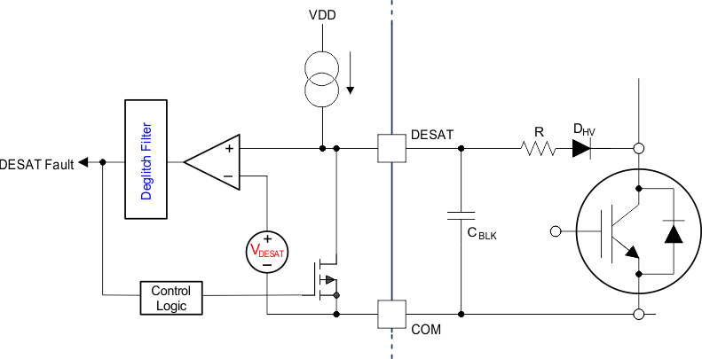
6.3.4 Desaturation (DESAT) Protection
The UCC5710x-Q1 implements a fast overcurrent and short circuit protection feature to protect the MOSFET/IGBT from catastrophic breakdown during fault. The DESAT pin has a typical 6.5 V threshold with respect to COM, the source or emitter of the power semiconductor. When the input is in a floating condition or the output is held in low state, the DESAT pin is pulled down by an internal MOSFET and held in the LOW state, which prevents the overcurrent and short circuit fault from false triggering. The internal current source of the DESAT pin is activated only during the driver ON state, which means the overcurrent and short circuit protection feature only works when the power semiconductor is in the ON state. The internal pulldown MOSFET helps to discharge the voltage of the DESAT pin when the power semiconductor is turned off. The features a 150-ns internal leading edge blanking time after the OUT switches to high state. The UCC5710x-Q1 internal current source is activated to charge the external blanking capacitor after the internal leading edge blanking time. The typical value of the internal current source is 250 µA.
 Figure 6-5 DESAT Protection