JAJSKM1C october 2019 – september 2021 UCC5870-Q1
PRODUCTION DATA
- 1
- 1 特長
- 2 アプリケーション
- 3 概要
- 4 Revision History
- 5 Pin Configuration and Functions
- 6 Specifications
-
7 Detailed Description
- 7.1 Overview
- 7.2 Functional Block Diagram
- 7.3
Feature Description
- 7.3.1 Power Supplies
- 7.3.2 Driver Stage
- 7.3.3 Integrated ADC for Front-End Analog (FEA) Signal Processing
- 7.3.4 Fault and Warning Classification
- 7.3.5
Diagnostic Features
- 7.3.5.1 Undervoltage Lockout (UVLO) and Overvoltage Lockout (OVLO)
- 7.3.5.2 CLAMP, OUTH, and OUTL Clamping Circuits
- 7.3.5.3 Active Miller Clamp
- 7.3.5.4 DESAT based Short Circuit Protection (DESAT)
- 7.3.5.5 Shunt Resistor based Overcurrent Protection (OCP) and Short Circuit Protection (SCP)
- 7.3.5.6 Temperature Monitoring and Protection for the Power Transistors
- 7.3.5.7 Active High Voltage Clamping (VCECLP)
- 7.3.5.8 Two-Level Turn-Off
- 7.3.5.9 Soft Turn-Off (STO)
- 7.3.5.10 Thermal Shutdown (TSD) and Temperature Warning (TWN) of Driver IC
- 7.3.5.11 Active Short Circuit Support (ASC)
- 7.3.5.12 Shoot-Through Protection (STP)
- 7.3.5.13 Gate Voltage Monitoring and Status Feedback
- 7.3.5.14 VGTH Monitor
- 7.3.5.15 Cyclic Redundancy Check (CRC)
- 7.3.5.16 Configuration Data CRC
- 7.3.5.17 SPI Transfer Write/Read CRC
- 7.3.5.18 TRIM CRC Check
- 7.4 Device Functional Modes
- 7.5 Programming
- 7.6 Register Maps
- 8 Applications and Implementation
- 9 Power Supply Recommendations
- 10Layout
- 11Device and Documentation Support
- 12Mechanical, Packaging, and Orderable Information
7.5.1.2 SPI Data Frame
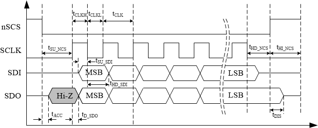
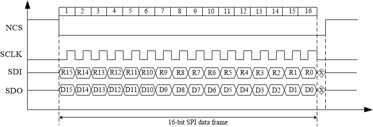
The SPI data frame is composed of 16bits. The timing scheme and format of a data frame is shown in Figure 7-43 and Figure 7-44.
 Figure 7-43 Timing scheme of SPI communication
 Figure 7-44 16-bit of SPI data frame.
The 16-bit data frame includes three data fields: chip address (CHIP_ADDR), command type (CMD), and an 8-bit data (DATA). The chip address (CHIP_ADDR) bits are used, regardless of the system configuration. However, when using the Daisy Chain or Independent Slave configurations, 0x0 or 0xF is used for all of the devices in the system. In Address-based configuration, the devices are individually addressed, and all devices respond to 0x0 and 0xF. Note that SDO is high impedance until it receives a command with the programmed device address. Once receiving the valid addressed command, the SDO is driven to send out data. When an invalid addressed command or 0xF (broadcast address) is received, the SDO returns to high impedance, thereby allowing other devices to take control of the shared MISO (SDO) bus. There are 10 command types used by the device, defined in Table 7-3.
| 16-BIT DATA FRAME | |||||||||||||||||
|---|---|---|---|---|---|---|---|---|---|---|---|---|---|---|---|---|---|
| BIT15 | BIT14 | BIT13 | BIT12 | BIT11 | BIT10 | BIT9 | BIT8 | BIT7 | BIT6 | BIT5 | BIT4 | BIT3 | BIT2 | BIT1 | BIT0 | ||
| Command Name | Command Description | CHIP_ADDR | CMD + DATA | ||||||||||||||
| DRV_EN | Driver output enable | CA[3] | CA[2] | CA[1] | CA[0] | 0 | 0 | 0 | 0 | 0 | 0 | 0 | 0 | 1 | 0 | 0 | 1 |
| DRV_DIS | Driver output disable | CA[3] | CA[2] | CA[1] | CA[0] | 0 | 0 | 0 | 0 | 0 | 0 | 0 | 0 | 1 | 0 | 1 | 0 |
| RD_DATA | Read data from register address RA[4:0] | CA[3] | CA[2] | CA[1] | CA[0] | 0 | 0 | 0 | 1 | 0 | 0 | 0 | RA[4] | RA[3] | RA[2] | RA[1] | RA[0] |
| CFG_IN | Enter configuration state | CA[3] | CA[2] | CA[1] | CA[0] | 0 | 0 | 1 | 0 | 0 | 0 | 1 | 0 | 0 | 0 | 1 | 0 |
| NOP | No operation | CA[3] | CA[2] | CA[1] | CA[0] | 0 | 1 | 0 | 1 | 0 | 1 | 0 | 0 | 0 | 0 | 1 | 0 |
| SW_RESET | Software RESET (Reinitialize the configurable registers) | CA[3] | CA[2] | CA[1] | CA[0] | 0 | 1 | 1 | 1 | 0 | 0 | 0 | 0 | 1 | 0 | 0 | 0 |
| WRH | Write D[15:8] to register RA[4:0] | CA[3] | CA[2] | CA[1] | CA[0] | 1 | 0 | 1 | 0 | D[15] | D[14] | D[13] | D[12] | D[11] | D[10] | D[9] | D[8] |
| WRL | Write D[7:0] to register RA[4:0] | CA[3] | CA[2] | CA[1] | CA[0] | 1 | 0 | 1 | 1 | D[7] | D[6] | D[5] | D[4] | D[3] | D[2] | D[1] | D[0] |
| WR_RA | Write register address RA[4:0] | CA[3] | CA[2] | CA[1] | CA[0] | 1 | 1 | 0 | 0 | 0 | 0 | 0 | RA[4] | RA[3] | RA[2] | RA[1] | RA[0] |
| WR_CA(1) | Write chip address CA[3:0] | 1 | 1 | 1 | 1 | 1 | 1 | 0 | 1 | 1 | 0 | 1 | 0 | CA[3] | CA[2] | CA[1] | CA[0] |