JAJSKM1C october   2019  – september 2021 UCC5870-Q1

PRODUCTION DATA  

  1.   1
  2. 特長
  3. アプリケーション
  4. 概要
  5. Revision History
  6. Pin Configuration and Functions
  7. Specifications
    1. 6.1  Absolute Maximum Ratings
    2. 6.2  ESD Ratings
    3. 6.3  Recommended Operating Conditions
    4. 6.4  Thermal Information
    5. 6.5  Power Ratings
    6. 6.6  Insulation Specifications
    7. 6.7  Electrical Characteristics
    8. 6.8  SPI Timing Requirements
    9. 6.9  Switching Characteristics
    10. 6.10 Typical Characteristics
  8. Detailed Description
    1. 7.1 Overview
    2. 7.2 Functional Block Diagram
    3. 7.3 Feature Description
      1. 7.3.1 Power Supplies
        1. 7.3.1.1 VCC1
        2. 7.3.1.2 VCC2
        3. 7.3.1.3 VEE2
        4. 7.3.1.4 VREG1
        5. 7.3.1.5 VREG2
        6. 7.3.1.6 VREF
        7. 7.3.1.7 Other Internal Rails
      2. 7.3.2 Driver Stage
      3. 7.3.3 Integrated ADC for Front-End Analog (FEA) Signal Processing
        1. 7.3.3.1 AI* Setup
        2. 7.3.3.2 ADC Setup and Sampling Modes
          1. 7.3.3.2.1 Center Sampling Mode
          2. 7.3.3.2.2 Edge Sampling Mode
          3. 7.3.3.2.3 Hybrid Mode
        3. 7.3.3.3 DOUT Functionality
      4. 7.3.4 Fault and Warning Classification
      5. 7.3.5 Diagnostic Features
        1. 7.3.5.1  Undervoltage Lockout (UVLO) and Overvoltage Lockout (OVLO)
          1. 7.3.5.1.1 Built-In Self Test (BIST)
            1. 7.3.5.1.1.1 Analog Built-In Self Test (ABIST)
            2. 7.3.5.1.1.2 Function BIST
            3. 7.3.5.1.1.3 Clock Monitor
              1. 7.3.5.1.1.3.1 Clock Monitor Built-In Self Test
        2. 7.3.5.2  CLAMP, OUTH, and OUTL Clamping Circuits
        3. 7.3.5.3  Active Miller Clamp
        4. 7.3.5.4  DESAT based Short Circuit Protection (DESAT)
        5. 7.3.5.5  Shunt Resistor based Overcurrent Protection (OCP) and Short Circuit Protection (SCP)
        6. 7.3.5.6  Temperature Monitoring and Protection for the Power Transistors
        7. 7.3.5.7  Active High Voltage Clamping (VCECLP)
        8. 7.3.5.8  Two-Level Turn-Off
        9. 7.3.5.9  Soft Turn-Off (STO)
        10. 7.3.5.10 Thermal Shutdown (TSD) and Temperature Warning (TWN) of Driver IC
        11. 7.3.5.11 Active Short Circuit Support (ASC)
        12. 7.3.5.12 Shoot-Through Protection (STP)
        13. 7.3.5.13 Gate Voltage Monitoring and Status Feedback
        14. 7.3.5.14 VGTH Monitor
        15. 7.3.5.15 Cyclic Redundancy Check (CRC)
          1. 7.3.5.15.1 Calculating CRC
        16. 7.3.5.16 Configuration Data CRC
        17. 7.3.5.17 SPI Transfer Write/Read CRC
          1. 7.3.5.17.1 SDI CRC Check
          2. 7.3.5.17.2 SDO CRC Check
        18. 7.3.5.18 TRIM CRC Check
    4. 7.4 Device Functional Modes
      1. 7.4.1 State 1: RESET
      2. 7.4.2 State 2: Configuration 1
      3. 7.4.3 State 3: Configuration 2
      4. 7.4.4 State 4: Active
    5. 7.5 Programming
      1. 7.5.1 SPI Communication
        1. 7.5.1.1 System Configuration of SPI Communication
          1. 7.5.1.1.1 Independent Slave Configuration
          2. 7.5.1.1.2 Daisy Chain Configuration
          3. 7.5.1.1.3 Address-based Configuration
        2. 7.5.1.2 SPI Data Frame
          1. 7.5.1.2.1 Writing a Register
          2. 7.5.1.2.2 Reading a Register
    6. 7.6 Register Maps
      1. 7.6.1 UCC5870 Registers
  9. Applications and Implementation
    1. 8.1 Application Information
      1. 8.1.1 Power Dissipation Considerations
      2. 8.1.2 Device Addressing
    2. 8.2 Typical Application Using Internal ADC Reference and Power FET Sense Current Monitoring
      1. 8.2.1 Design Requirements
      2. 8.2.2 Detailed Design Procedure
        1. 8.2.2.1 VCC1, VCC2, and VEE2 Bypass Capacitors
        2. 8.2.2.2 VREF, VREG1, and VREG2 Bypass Capacitors
        3. 8.2.2.3 Bootstrap Capacitor (VBST)
        4. 8.2.2.4 VCECLP Input
        5. 8.2.2.5 External CLAMP Output
        6. 8.2.2.6 AI* Inputs
        7. 8.2.2.7 OUTH/ OUTL Outputs
        8. 8.2.2.8 nFLT* Outputs
      3. 8.2.3 Application Curves
    3. 8.3 Typical Application Using DESAT Power FET Monitoring
      1. 8.3.1 Detailed Design Procedure
        1. 8.3.1.1 DESAT Input
      2. 8.3.2 Application Curves
  10. Power Supply Recommendations
    1. 9.1 VCC1 Power Supply
    2. 9.2 VCC2 Power Supply
    3. 9.3 VEE2 Power Supply
    4. 9.4 VREF Supply (Optional)
  11. 10Layout
    1. 10.1 Layout Guidelines
      1. 10.1.1 Component Placement
      2. 10.1.2 Grounding Considerations
      3. 10.1.3 High-Voltage Considerations
      4. 10.1.4 Thermal Considerations
    2. 10.2 Layout Example
  12. 11Device and Documentation Support
    1. 11.1 Documentation Support
      1. 11.1.1 Related Documentation
    2. 11.2 Receiving Notification of Documentation Updates
    3. 11.3 サポート・リソース
    4. 11.4 Trademarks
    5. 11.5 静電気放電に関する注意事項
    6. 11.6 用語集
  13. 12Mechanical, Packaging, and Orderable Information

パッケージ・オプション

メカニカル・データ(パッケージ|ピン)
サーマルパッド・メカニカル・データ
発注情報

Two-Level Turn-Off

The two-level turn-off (2LTOFF) function limits the transistor current during shutoff during certain fault conditions. The 2LTOFF function is enabled for PS_OC, PS_SC, PS_TSD, and/or DESAT faults using the CF5[2LTOFF_STO_EN] bits (CFG5). When 2LTOFF is triggered, the gate of the power transistor is controlled to operate the transistor in the linear region where the channel current is controlled by the voltage level on the gate terminal. The power transistor current is reduced by controlling the gate voltage to a intermediate voltage, or plateau voltage, (V2LOFF) for t2LOFF, and then ramping the gate down to turn the power transistor off. While 2LTOFF is active, OUTL sinks current to discharge the gate capacitor of the power switch to the plateau voltage. The gate discharge current is programmable using the CFG8[GD_2LOFF_CURR] bits (CFG8). The plateau voltage level and duration are configured using the CFG8[GD_2LOFF_VOLT] and CFG8[GD_2LOFF_TIME] bits (CFG8), respectively. After holding the plateau voltage for the programmed time, the gate is discharged fully using the soft turn-off current or pulled low as normal with the OUTL driver. Enable the soft turn off current using the CFG8[GD_2LOFF_STO_EN] bit (CFG8). The implementation diagram and timing scheme are presented in Figure 7-24 and Figure 7-25, respectively.
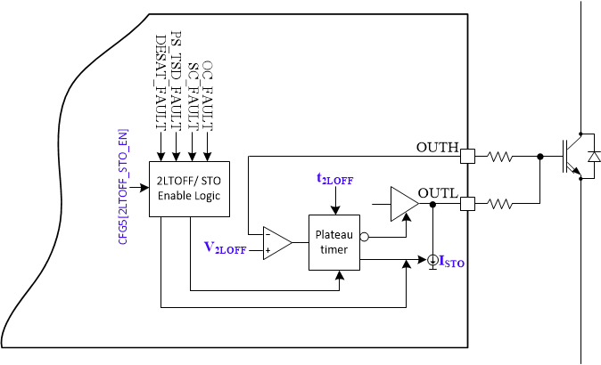
GUID-51A239AD-43BB-4AA9-AF1B-E7A5F82CF657-low.png Figure 7-24 Block diagram of implementation of two-level turn-off function
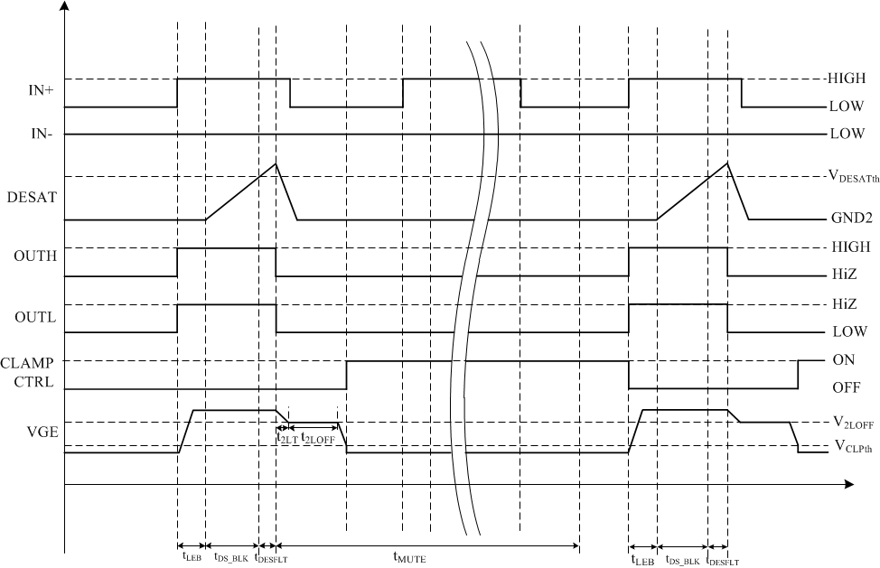
GUID-DA05ADB4-840B-4150-8E26-DC6EFE76B0DB-low.gif Figure 7-25 Timing scheme of implementation of two-level turn-off function