JAJSK73J March   2012  – November 2021 UCD3138

PRODUCTION DATA  

  1. 特長
  2. アプリケーション
  3. 概要
  4. 機能ブロック図
  5. Revision History
  6. Device Comparison Table
    1. 6.1 Product Family Comparison
    2. 6.2 Product Selection Matrix
  7. Pin Configuration and Functions
    1. 7.1 UCD3138RGC 64 QFN Pin Attributes
    2. 7.2 UCD3138RHA, UCD3138RMH and UCD3138RJA Pin Attributes
  8. Specifications
    1. 8.1 Absolute Maximum Ratings
    2. 8.2 ESD Ratings
    3. 8.3 Recommended Operating Conditions
    4. 8.4 Thermal Information
    5. 8.5 Electrical Characteristics
    6. 8.6 Timing and Switching Characteristics
    7. 8.7 Power Supply Sequencing
    8. 8.8 Peripherals
      1. 8.8.1 Digital Power Peripherals (DPPs)
        1. 8.8.1.1 Front End
        2. 8.8.1.2 DPWM Module
        3. 8.8.1.3 DPWM Events
        4. 8.8.1.4 High Resolution DPWM
        5. 8.8.1.5 Oversampling
        6. 8.8.1.6 DPWM Interrupt Generation
        7. 8.8.1.7 DPWM Interrupt Scaling/Range
    9. 8.9 Typical Temperature Characteristics
  9. Detailed Description
    1. 9.1 Overview
    2. 9.2 ARM Processor
    3. 9.3 Memory
      1. 9.3.1 CPU Memory Map and Interrupts
      2. 9.3.2 Boot ROM
      3. 9.3.3 Customer Boot Program
      4. 9.3.4 Flash Management
    4. 9.4 System Module
      1. 9.4.1 Address Decoder (DEC)
      2. 9.4.2 Memory Management Controller (MMC)
      3. 9.4.3 System Management (SYS)
      4. 9.4.4 Central Interrupt Module (CIM)
    5. 9.5 Feature Description
      1. 9.5.1  Sync FET Ramp and IDE Calculation
      2. 9.5.2  Automatic Mode Switching
        1. 9.5.2.1 Phase Shifted Full Bridge Example
        2. 9.5.2.2 LLC Example
        3. 9.5.2.3 Mechanism for Automatic Mode Switching
      3. 9.5.3  DPWMC, Edge Generation, IntraMux
      4. 9.5.4  Filter
        1. 9.5.4.1 Loop Multiplexer
        2. 9.5.4.2 Fault Multiplexer
      5. 9.5.5  Communication Ports
        1. 9.5.5.1 SCI (UART) Serial Communication Interface
        2. 9.5.5.2 PMBUS
        3. 9.5.5.3 General Purpose ADC12
        4. 9.5.5.4 Timers
          1. 9.5.5.4.1 24-bit PWM Timer
          2. 9.5.5.4.2 16-Bit PWM Timers
          3. 9.5.5.4.3 Watchdog Timer
      6. 9.5.6  Miscellaneous Analog
      7. 9.5.7  Package ID Information
      8. 9.5.8  Brownout
      9. 9.5.9  Global I/O
      10. 9.5.10 Temperature Sensor Control
      11. 9.5.11 I/O Mux Control
      12. 9.5.12 Current Sharing Control
      13. 9.5.13 Temperature Reference
    6. 9.6 Device Functional Modes
      1. 9.6.1 Normal Mode
      2. 9.6.2 Phase Shifting
      3. 9.6.3 DPWM Multiple Output Mode
      4. 9.6.4 DPWM Resonant Mode
      5. 9.6.5 Triangular Mode
      6. 9.6.6 Leading Edge Mode
  10. 10Application and Implementation
    1. 10.1 Application Information
    2. 10.2 Typical Application
      1. 10.2.1 Design Requirements
      2. 10.2.2 Detailed Design Procedure
        1. 10.2.2.1 PCMC (Peak Current Mode Control) PSFB (Phase Shifted Full Bridge) Hardware Configuration Overview
        2. 10.2.2.2 DPWM Initialization for PSFB
        3. 10.2.2.3 DPWM Synchronization
        4. 10.2.2.4 Fixed Signals to Bridge
        5. 10.2.2.5 Dynamic Signals to Bridge
        6. 10.2.2.6 System Initialization for PCM
          1. 10.2.2.6.1 Use of Front Ends and Filters in PSFB
          2. 10.2.2.6.2 Peak Current Detection
          3. 10.2.2.6.3 Peak Current Mode (PCM)
      3. 10.2.3 Application Curves
  11. 11Power Supply Recommendations
    1. 11.1 Introduction To Power Supply and Layout Recommendations
    2. 11.2 3.3-V Supply Pins
    3. 11.3 Recommendation for V33 Ramp up Slew Rate for UCD3138 and UCD3138064
    4. 11.4 Recommendation for RC Time Constant of RESET Pin for UCD3138 and UCD3138064
  12. 12Layout
    1. 12.1 Layout Guidelines
      1. 12.1.1 EMI and EMC Mitigation Guidelines
      2. 12.1.2 BP18 Pin
      3. 12.1.3 Additional Bias Guidelines
      4. 12.1.4 UCD3138 Pin Connection Recommendation
        1. 12.1.4.1 Current Amplifier With EADC Connection
        2. 12.1.4.2 DPWM Synchronization
        3. 12.1.4.3 GPIOS
        4. 12.1.4.4 DPWM PINS
        5. 12.1.4.5 EAP and EAN Pins
        6. 12.1.4.6 ADC Pins
      5. 12.1.5 UART Communication Port
      6. 12.1.6 Special Considerations
    2. 12.2 Layout Example
      1. 12.2.1 UCD3138 and UCD3138064 40 Pin
      2. 12.2.2 UCD3138 and UCD3138064 64 Pin
  13. 13Device and Documentation Support
    1. 13.1 Device Support
      1. 13.1.1 Code Composer Studio
      2. 13.1.2 Tools and Documentation
    2. 13.2 Documentation Support
      1. 13.2.1 References
    3. 13.3 Receiving Notification of Documentation Updates
    4. 13.4 サポート・リソース
    5. 13.5 Trademarks
    6. 13.6 Electrostatic Discharge Caution
    7. 13.7 Glossary
  14. 14Mechanical Packaging and Orderable Information
    1. 14.1 Packaging Information

パッケージ・オプション

メカニカル・データ(パッケージ|ピン)
サーマルパッド・メカニカル・データ
発注情報

Recommendation for RC Time Constant of RESET Pin for UCD3138 and UCD3138064

Ideally, the ARM core should begin execution of ROM code only after V33>3V. The ROM code reads trim values and loads trim registers. Lack of sufficient voltage during this operation can result in unexpected device functioning. Depending on V33 slew rate, the duration for which there is insufficient voltage on V33 is varied. During this time, a reliable trim operation is not ensured. Applying an RC filter between V33 and the RESET pin can increase the delay from V33 power up to the device coming out of reset.
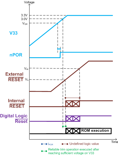
GUID-50FDF2B8-24CB-4995-BF04-9D3015B14E00-low.png Figure 11-2 Recommended Timing Diagram of V33 and RESET for UCD3138 and UCD3138064

Example Solution:

If the V33 supply slew rate is 0.6 V/ms, then the minimum τ required is calculated as follows:

Equation 2. GUID-D6D958D8-5EE2-45A9-8194-6700D6659768-low.gif
Equation 3. GUID-070B4E0C-6BD2-4315-8571-DA59C4657143-low.gif

If R and C are 2.21 k and 2.2 uF, then τ evaluates as:

Equation 4. GUID-C4FD0972-0A8C-4AC5-8261-6D163BDA8868-low.gif

These values of 2.21 kΩ and 2.2 µF will ensure that the RESET will be a logic-0 until V33 crosses 3V. [τ > τRESET_MIN]