JAJSK73J March 2012 – November 2021 UCD3138
PRODUCTION DATA
- 1 特長
- 2 アプリケーション
- 3 概要
- 4 機能ブロック図
- 5 Revision History
- 6 Device Comparison Table
- 7 Pin Configuration and Functions
- 8 Specifications
-
9 Detailed Description
- 9.1 Overview
- 9.2 ARM Processor
- 9.3 Memory
- 9.4 System Module
- 9.5
Feature Description
- 9.5.1 Sync FET Ramp and IDE Calculation
- 9.5.2 Automatic Mode Switching
- 9.5.3 DPWMC, Edge Generation, IntraMux
- 9.5.4 Filter
- 9.5.5 Communication Ports
- 9.5.6 Miscellaneous Analog
- 9.5.7 Package ID Information
- 9.5.8 Brownout
- 9.5.9 Global I/O
- 9.5.10 Temperature Sensor Control
- 9.5.11 I/O Mux Control
- 9.5.12 Current Sharing Control
- 9.5.13 Temperature Reference
- 9.6 Device Functional Modes
-
10Application and Implementation
- 10.1 Application Information
- 10.2
Typical Application
- 10.2.1 Design Requirements
- 10.2.2 Detailed Design Procedure
- 10.2.3 Application Curves
- 11Power Supply Recommendations
- 12Layout
- 13Device and Documentation Support
- 14Mechanical Packaging and Orderable Information
パッケージ・オプション
メカニカル・データ(パッケージ|ピン)
サーマルパッド・メカニカル・データ
発注情報
11.3 Recommendation for V33 Ramp up Slew Rate for UCD3138 and UCD3138064
UCD3138 and UCD3138064 need a 2.2-µF pullup capacitor from BP18 to V33 as described before. Capacitors with a value of 2.2 µF and 1 µF create a capacitor divider which pull BP18 up as V33 rises. Ensure that as V33 rises, the slew rate is not fast enough to cause BP18 to overshoot, resulting in a reliability issue. TI requires that the maximum voltage of BP18 does not exceed 1.95 V. By calculation, if V33 ramps up linearly, the maximum V33 slew rate should be less than 6 V/ms.
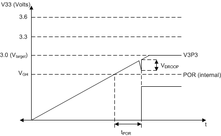
Also, the internal BP18 regulator is enabled when V33 is higher than VGH and POR is activated. V33 charges the capacitor of BP18 through the internal regulator. This charge causes a voltage dip in the V33 pin as shown in Figure 11-1 and the charge may trigger a V33 undervoltage (POR) event, causing a chip reset. To prevent POR trigger signal oscillation and successive chip resets, TI recommends a minimum slew rate of 2.6 V/ms.
 Figure 11-1 V33 Voltage Dip When POR is Activated
From the Figure 11-1 recommendations, the slew rate using the 2.2 uF/1uF capacitor combination requires that the slew rate must be as follows:
