JAJSHD5D November 2010 – April 2019 UCD90160
PRODUCTION DATA.
- 1 特長
- 2 アプリケーション
- 3 概要
- 4 改訂履歴
- 5 概要(続き)
- 6 Pin Configuration and Functions
- 7 Specifications
-
8 Detailed Description
- 8.1 Overview
- 8.2 Functional Block Diagram
- 8.3 Feature Description
- 8.4
Device Functional Modes
- 8.4.1 Power-Supply Sequencing
- 8.4.2 Pin-Selected Rail States
- 8.4.3 Voltage Monitoring
- 8.4.4 Fault Responses and Alert Processing
- 8.4.5 Shut Down All Rails and Sequence On (Resequence)
- 8.4.6 GPIOs
- 8.4.7 GPO Control
- 8.4.8 GPO Dependencies
- 8.4.9 GPI Special Functions
- 8.4.10 Power-Supply Enables
- 8.4.11 Cascading Multiple Devices
- 8.4.12 PWM Outputs
- 8.4.13 Programmable Multiphase PWMs
- 8.4.14 Margining
- 8.4.15 System Reset Signal
- 8.4.16 Watch Dog Timer
- 8.4.17 Run Time Clock
- 8.4.18 Data and Error Logging to Flash Memory
- 8.4.19 Brownout Function
- 8.4.20 PMBus Address Selection
- 8.5 Programming
- 9 Application and Implementation
- 10Power Supply Recommendations
- 11Layout
- 12デバイスおよびドキュメントのサポート
- 13メカニカル、パッケージ、および注文情報
パッケージ・オプション
メカニカル・データ(パッケージ|ピン)
- RGC|64
サーマルパッド・メカニカル・データ
- RGC|64
発注情報
8.4.3 Voltage Monitoring
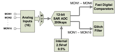
Up to 16 voltages can be monitored using the analog input pins. The input voltage range is 0 V–2.5 V for MON pins 1-6, 55-59, 62, and 63. Pins 50, 52, and 54 can measure down to 0.2 V.
The ADC operates continuously, requiring 3.89 μs to convert a single analog input. Each rail is sampled by the sequencing and monitoring algorithm every 400 μs. The maximum source impedance of any sampled voltage should be less than 4 kΩ. The source impedance limit is particularly important when a resistor-divider network is used to lower the voltage applied to the analog input pins.
MON1 - MON6 can be configured using digital hardware comparators, which can be used to achieve faster fault responses. Each hardware comparator has four thresholds (two UV (Fault and Warning) and two OV (Fault and Warning)). The hardware comparators respond to UV or OV conditions in about 80 μs (faster than 400 µs for the ADC inputs) and can be used to disable rails or assert GPOs. The only fault response available for the hardware comparators is to shut down immediately.
An internal 2.5-V reference is used by the ADC. The ADC reference has a tolerance of ±0.5% between 0°C and 125°C and a tolerance of ±1% between –40°C and 125°C. An external voltage divider is required for monitoring voltages higher than 2.5 V. The nominal rail voltage and the external scale factor can be entered into the Fusion GUI and are used to report the actual voltage being monitored instead of the ADC input voltage. The nominal voltage is used to set the range and precision of the reported voltage according to Table 2.
 Figure 12. Voltage Monitoring Block Diagram
 Table 2. Voltage Range and Resolution
| VOLTAGE RANGE
(Volts) |
RESOLUTION
(millivolts) |
|---|---|
| 0 to 127.99609 | 3.90625 |
| 0 to 63.99805 | 1.95313 |
| 0 to 31.99902 | 0.97656 |
| 0 to 15.99951 | 0.48824 |
| 0 to 7.99976 | 0.24414 |
| 0 to 3.99988 | 0.12207 |
| 0 to 1.99994 | 0.06104 |
| 0 to 0.99997 | 0.03052 |
Although the monitor results can be reported with a resolution of about 15 μV, the real conversion resolution of 610 μV is fixed by the 2.5-V reference and the 12-bit ADC.