JAJSHD5D November 2010 – April 2019 UCD90160
PRODUCTION DATA.
- 1 特長
- 2 アプリケーション
- 3 概要
- 4 改訂履歴
- 5 概要(続き)
- 6 Pin Configuration and Functions
- 7 Specifications
-
8 Detailed Description
- 8.1 Overview
- 8.2 Functional Block Diagram
- 8.3 Feature Description
- 8.4
Device Functional Modes
- 8.4.1 Power-Supply Sequencing
- 8.4.2 Pin-Selected Rail States
- 8.4.3 Voltage Monitoring
- 8.4.4 Fault Responses and Alert Processing
- 8.4.5 Shut Down All Rails and Sequence On (Resequence)
- 8.4.6 GPIOs
- 8.4.7 GPO Control
- 8.4.8 GPO Dependencies
- 8.4.9 GPI Special Functions
- 8.4.10 Power-Supply Enables
- 8.4.11 Cascading Multiple Devices
- 8.4.12 PWM Outputs
- 8.4.13 Programmable Multiphase PWMs
- 8.4.14 Margining
- 8.4.15 System Reset Signal
- 8.4.16 Watch Dog Timer
- 8.4.17 Run Time Clock
- 8.4.18 Data and Error Logging to Flash Memory
- 8.4.19 Brownout Function
- 8.4.20 PMBus Address Selection
- 8.5 Programming
- 9 Application and Implementation
- 10Power Supply Recommendations
- 11Layout
- 12デバイスおよびドキュメントのサポート
- 13メカニカル、パッケージ、および注文情報
パッケージ・オプション
メカニカル・データ(パッケージ|ピン)
- RGC|64
サーマルパッド・メカニカル・データ
- RGC|64
発注情報
8.4.8 GPO Dependencies
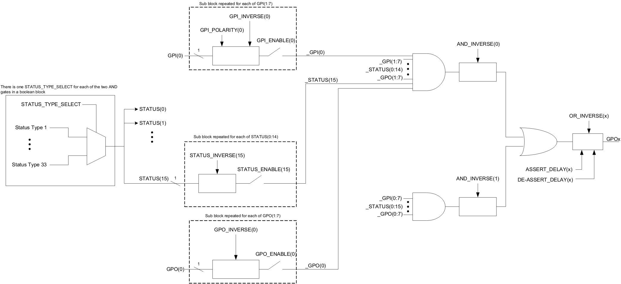
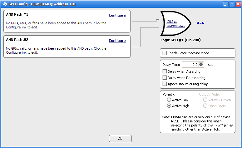
GPIOs can be configured as outputs that are based on Boolean combinations of up to two ANDs, all ORed together (Figure 15). Inputs to the logic blocks can include the first 8 defined GPOs, GPIs and rail-status flags. One rail status type is selectable as an input for each AND gate in a Boolean block. For a selected rail status, the status flags of all active rails can be included as inputs to the AND gate. _LATCH rail-status types stay asserted until cleared by a MFR PMBus command or by a specially configured GPI pin. The different rail-status types are shown in Table 4. See the UCD90xxx Sequencer and System Health Controller PMBus Command Reference for complete definitions of rail-status types. The GPO response can be configured to have a delayed assertion or deassertion.
 Figure 15. Boolean Logic Combinations
  Figure 16. Fusion Boolean Logic Builder
 Table 4. Rail-Status Types for Boolean Logic
| Rail-Status Types | ||
|---|---|---|
| POWER_GOOD | TON_MAX_FAULT | VOUT_UV_WARN_LATCH |
| MARGIN_EN | TOFF_MAX_WARN | VOUT_UV_FAULT_LATCH |
| MRG_LOW_nHIGH | SEQ_ON_TIMEOUT | TON_MAX_FAULT_LATCH |
| VOUT_OV_FAULT | SEQ_OFF_TIMEOUT | TOFF_MAX_WARN_LATCH |
| VOUT_OV_WARN | SYSTEM_WATCHDOG_TIMEOUT | SEQ_ON_TIMEOUT_LATCH |
| VOUT_UV_WARN | VOUT_OV_FAULT_LATCH | SEQ_OFF_TIMEOUT_LATCH |
| VOUT_UV_FAULT | VOUT_OV_WARN_LATCH | SYSTEM_WATCHDOG_TIMEOUT_LATCH |