JAJSFV7C September 2016 – March 2020 UCD90160A
PRODUCTION DATA.
- 1 特長
- 2 アプリケーション
- 3 概要
- 4 改訂履歴
- 5 概要 (続き)
- 6 Pin Configuration and Functions
- 7 Specifications
-
8 Detailed Description
- 8.1 Overview
- 8.2 Functional Block Diagram
- 8.3 Feature Description
- 8.4
Device Functional Modes
- 8.4.1 Power Supply Sequencing
- 8.4.2 Pin-Selected Rail States
- 8.4.3 Voltage Monitoring
- 8.4.4 Fault Responses and Alert Processing
- 8.4.5 Shut Down All Rails and Sequence On (Resequence)
- 8.4.6 GPIOs
- 8.4.7 GPO Control
- 8.4.8 GPO Dependencies
- 8.4.9 GPI Special Functions
- 8.4.10 Power Supply Enables
- 8.4.11 Cascading Multiple Devices
- 8.4.12 PWM Outputs
- 8.4.13 Programmable Multiphase PWMs
- 8.4.14 Margining
- 8.4.15 System Reset Signal
- 8.4.16 Watch Dog Timer
- 8.4.17 Run Time Clock
- 8.4.18 Data and Error Logging to Flash Memory
- 8.4.19 Brownout Function
- 8.4.20 PMBus Address Selection
- 8.4.21 Device Reset
- 8.5 Programming
- 9 Application and Implementation
- 10Power Supply Recommendations
- 11Layout
- 12デバイスおよびドキュメントのサポート
- 13メカニカル、パッケージ、および注文情報
パッケージ・オプション
メカニカル・データ(パッケージ|ピン)
- RGC|64
サーマルパッド・メカニカル・データ
- RGC|64
発注情報
8.4.14.2 Closed-Loop Margining
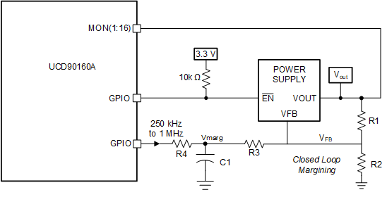
Closed-loop margining uses a PWM or FPWM output for each power supply that is being margined. An external RC network converts the FPWM pulse train into a DC margining voltage. The margining voltage is connected to the appropriate power supply feedback node through a resistor. The power supply output voltage is monitored, and the margining voltage is controlled by adjusting the PWM duty cycle until the power supply output voltage reaches the margin-low and margin-high voltages set by the user. The voltage setting resolutions will be the same that applies to the voltage measurement resolution (Table 3). The closed loop margining can operate in several modes (Table 8). Given that this closed-loop system has feed back through the ADC, the closed-loop margining accuracy will be dominated by the ADC measurement. The relationship between duty cycle and margined voltage is configurable so that voltage increases when duty cycle increases or decreases. For more details on configuring the UCD90160A for margining, see the Voltage Margining Using the UCD9012x application note (SLVA375).
Table 8. Closed Loop Margining Modes
| MODE | DESCRIPTION |
|---|---|
| DISABLE | Margining is disabled. |
| ENABLE_TRI_STATE | When not margining, the PWM pin is set to high impedance state. |
| ENABLE_ACTIVE_TRIM | When not margining, the PWM duty-cycle is continuously adjusted to keep the voltage at VOUT_COMMAND. |
| ENABLE_FIXED_DUTY_CYCLE | When not margining, the PWM duty-cycle is set to a fixed duty-cycle. |
 Figure 24. Closed-Loop Margining