JAJSHD6B August 2016 – May 2019 UCD90320
PRODUCTION DATA.
- 1 特長
- 2 アプリケーション
- 3 概要
- 4 改訂履歴
- 5 概要(続き)
- 6 Pin Configuration and Functions
- 7 Specifications
-
8 Detailed Description
- 8.1 Overview
- 8.2 Functional Block Diagram
- 8.3 Feature Description
- 8.4
Device Functional Modes
- 8.4.1 Rail Monitoring Configuration
- 8.4.2 GPI Configuration
- 8.4.3 Rail Sequence Configuration
- 8.4.4 Fault Responses Configuration
- 8.4.5 GPO Configuration
- 8.4.6 Margining Configuration
- 8.4.7 Pin Selected Rail States Configuration
- 8.4.8 Watchdog Timer
- 8.4.9 System Reset Function
- 8.4.10 Cascading Multiple Devices
- 8.4.11 Rail Monitoring
- 8.4.12 Status Monitoring
- 8.4.13 Data and Error Logging to EEPROM Memory
- 8.4.14 Black Box First Fault Logging
- 8.4.15 PMBus Address Selection
- 8.4.16 ADC Reference
- 8.4.17 Device Reset
- 8.4.18 Brownout
- 8.4.19 Internal Fault Management
- 8.5 Device Configuration and Programming
- 9 Application and Implementation
- 10Power Supply Recommendations
- 11Layout
- 12デバイスおよびドキュメントのサポート
- 13メカニカル、パッケージ、および注文情報
8.4.11 Rail Monitoring
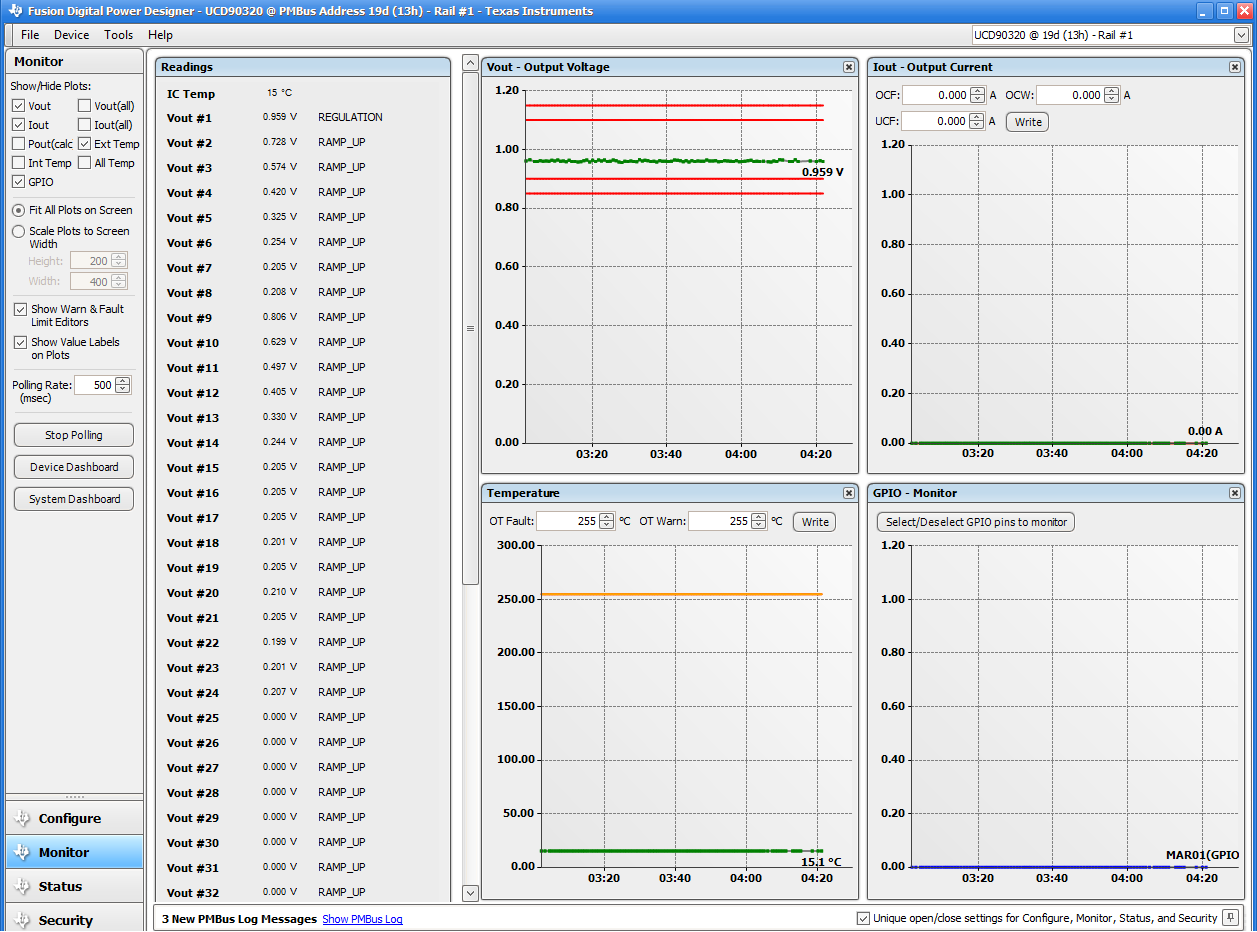
UCD90320 monitors up to 24 analog inputs including voltages, current, and temperature and eight digital inputs for POWER_GOOD. Use either the Fusion GUI or a PMBus interface host to poll data from UCD90320. The Fusion GUI displays monitored rail voltage, current, and temperature information on the Monitor page, as shown in Figure 31. Use polling to debug system-level issues.
 Figure 31. Fusion Digital Power Designer software Monitor Page
 Table 4. Rail State Value Descriptions
| RAIL STATE | VALUE | CONDITION FOR ENTERING RAIL STATE |
|---|---|---|
| IDLE | 1 | When a turn-ON condition is not met, or when rail is shut down due to a fault, or when the rail is waiting for the turn-ON period to resequence |
| SEQ_ON | 2 | Waits for the dependency to be met to assert the enable signal |
| START_DELAY | 3 | TON_DELAY to assert the enable signal |
| RAMP_UP | 4 | Enable signal is asserted and rail is approaching the power good threshold. If the power good threshold is set to 0 V, the rail stays at this state even if the monitored voltage is higher than 0 V. |
| REGULATION | 5 | When the monitoring voltage is higher than the power good threshold when the enable signal is asserted, rails stay at this state even if the voltage is below the power good threshold and continues as long as there is no fault action taken. |
| SEQ_OFF | 6 | Wait for the dependency to be met to de-assert the enable signal |
| STOP_DELAY | 7 | TOFF_DELAY to de-assert the enable signal |
| RAMP_DOWN | 8 | The enable signal is de-asserted and rail is ramping down. This state is available only if TOFF_MAX_WARN_LIMIT is not set to unlimited, or if the turn-off sequence is triggered by a fault action. The rail must not be under fault retry sequence to show this RAMP_DOWN state. Otherwise, the IDLE state is present. |