JAJSHD6B August 2016 – May 2019 UCD90320
PRODUCTION DATA.
- 1 特長
- 2 アプリケーション
- 3 概要
- 4 改訂履歴
- 5 概要(続き)
- 6 Pin Configuration and Functions
- 7 Specifications
-
8 Detailed Description
- 8.1 Overview
- 8.2 Functional Block Diagram
- 8.3 Feature Description
- 8.4
Device Functional Modes
- 8.4.1 Rail Monitoring Configuration
- 8.4.2 GPI Configuration
- 8.4.3 Rail Sequence Configuration
- 8.4.4 Fault Responses Configuration
- 8.4.5 GPO Configuration
- 8.4.6 Margining Configuration
- 8.4.7 Pin Selected Rail States Configuration
- 8.4.8 Watchdog Timer
- 8.4.9 System Reset Function
- 8.4.10 Cascading Multiple Devices
- 8.4.11 Rail Monitoring
- 8.4.12 Status Monitoring
- 8.4.13 Data and Error Logging to EEPROM Memory
- 8.4.14 Black Box First Fault Logging
- 8.4.15 PMBus Address Selection
- 8.4.16 ADC Reference
- 8.4.17 Device Reset
- 8.4.18 Brownout
- 8.4.19 Internal Fault Management
- 8.5 Device Configuration and Programming
- 9 Application and Implementation
- 10Power Supply Recommendations
- 11Layout
- 12デバイスおよびドキュメントのサポート
- 13メカニカル、パッケージ、および注文情報
8.4.18 Brownout
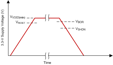
The UCD90320 device triggers brownout event when the V33D pin voltage drops below the brownout threshold voltage, (VBOR). During a brownout event, the device continues to write fault logs into the EEPROM that occurred before the brownout event. As the supply voltage continues to drop, the device fully shuts down when the V33D pin voltage is below the shutdown threshold voltage (VSHDN). Any fault event that has not been written into the EEPROM before the device shutdown is lost.
In the scenario where several faults happen immediately before the brownout event, the device requires a capacitance of 500 µs in order to write the first fault event into the EEPROM. The write function requires an additional 4 ms to write the Black Box fault log into the EEPROM. Therefore, in order to preserve at least the first fault log, user must provide enough local capacitance to maintain the V33D rail above VSHDN for 500 µs (or 4.5ms with the Black Box fault log). Longer holdup time allows more fault events to be written into the EEPROM during brownout.
NOTE
The hold-up time is affected by V33D rail capacitance, the UCD90320 supply current and external circuits that source current from the rail (such as LEDs, load current on I/O pins, and other devices powered by the same rail).
 Figure 36. Reset and Brownout Thresholds