SLVS813C June   2008  – November 2016 UCD9081

PRODUCTION DATA.  

  1. Features
  2. Applications
  3. Description
  4. Revision History
  5. Pin Configuration and Functions
  6. Specifications
    1. 6.1 Absolute Maximum Ratings
    2. 6.2 Recommended Operating Conditions
    3. 6.3 Thermal Information
    4. 6.4 Electrical Characteristics
    5. 6.5 Timing Requirements: I2C Interface
    6. 6.6 Typical Characteristics
  7. Parameter Measurement Information
  8. Detailed Description
    1. 8.1 Overview
    2. 8.2 Functional Block Diagram
    3. 8.3 Feature Description
      1. 8.3.1 Rail Configuration
      2. 8.3.2 Graphical User Interface (GUI)
    4. 8.4 Device Functional Modes
      1. 8.4.1  Power Supply Sequencing
      2. 8.4.2  Power-Supply Enables
      3. 8.4.3  General-Purpose Outputs
      4. 8.4.4  Device Reset
      5. 8.4.5  Voltage Reference
      6. 8.4.6  Voltage Monitoring
      7. 8.4.7  Rail Shutdown
      8. 8.4.8  Alarm Processing
        1. 8.4.8.1 Ignore
        2. 8.4.8.2 Log Only
        3. 8.4.8.3 Retry n Times
        4. 8.4.8.4 Retry Continuously
        5. 8.4.8.5 Sequence
        6. 8.4.8.6 Sequence After Shutdown
      9. 8.4.9  Error Logging
      10. 8.4.10 Brownout
    5. 8.5 Programming
      1. 8.5.1 I2C Interface
      2. 8.5.2 Configuring and Monitoring the UCD9081
      3. 8.5.3 Resetting the Flash Error Log
      4. 8.5.4 Configuring the UCD9081
      5. 8.5.5 User Data
      6. 8.5.6 I2C Address Selection
      7. 8.5.7 I2C Transactions
        1. 8.5.7.1 I2C Unidirectional Transfer
        2. 8.5.7.2 I2C Combined Format
    6. 8.6 Register Maps
      1. 8.6.1  Register Descriptions
      2. 8.6.2  RAIL
      3. 8.6.3  ERROR
      4. 8.6.4  STATUS
      5. 8.6.5  VERSION
      6. 8.6.6  RAILSTATUS
      7. 8.6.7  FLASHLOCK
      8. 8.6.8  RESTART
      9. 8.6.9  WADDR and WDATA
      10. 8.6.10 Reading the FLASH Error Log
  9. Application and Implementation
    1. 9.1 Application Information
      1. 9.1.1 Considerations for MONX Input Series Resistance, RS
      2. 9.1.2 Estimating UCD9081 Reporting Accuracy Over Variations in ADC Voltage Reference
    2. 9.2 Typical Application
      1. 9.2.1 Design Requirements
      2. 9.2.2 Detailed Design Procedure
      3. 9.2.3 Application Curve
  10. 10Power Supply Recommendations
  11. 11Layout
    1. 11.1 Layout Guidelines
    2. 11.2 Layout Example
  12. 12Device and Documentation Support
    1. 12.1 Documentation Support
      1. 12.1.1 Related Documentation
    2. 12.2 Receiving Notification of Documentation Updates
    3. 12.3 Community Resources
    4. 12.4 Trademarks
    5. 12.5 Electrostatic Discharge Caution
    6. 12.6 Glossary
  13. 13Mechanical, Packaging, and Orderable Information

パッケージ・オプション

メカニカル・データ(パッケージ|ピン)
サーマルパッド・メカニカル・データ
発注情報

Layout

Layout Guidelines

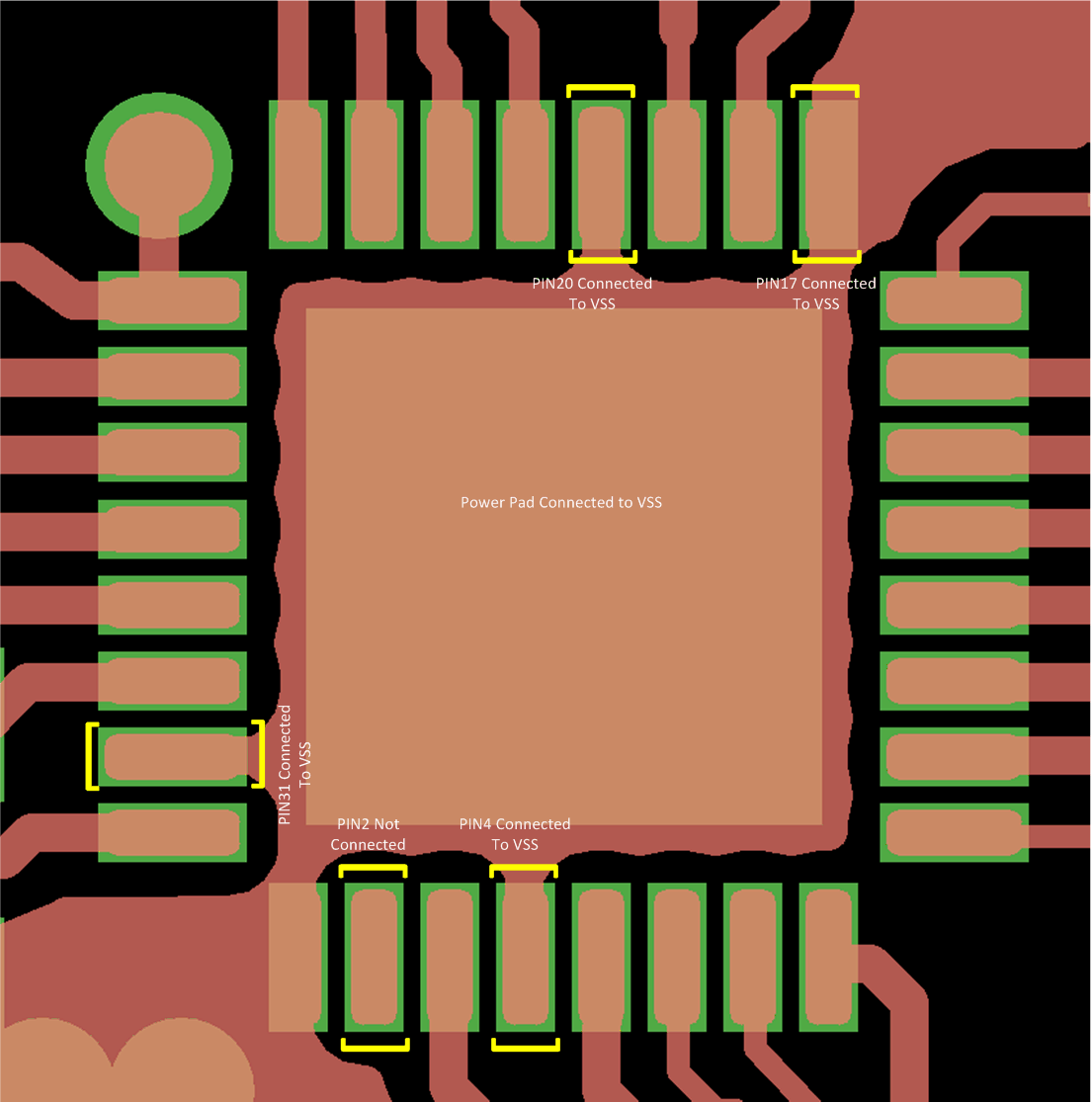
The power pad provides a thermal and mechanical interface between the device and the printed-circuit board (PCB). Connect the power pad to the device VSS pins. Pin 2 must not be connected. Pin (4, 17, 20, 31) are recommended to connect to VSS because these pins are not connected internally.

Layout Example

UCD9081 Layout_example_Top_Layer.gif Figure 22. UCD9081 Layout, Top Layer