SBOS275G June 2003 – December 2015 VCA810
PRODUCTION DATA.
- 1 Features
- 2 Applications
- 3 Description
- 4 Revision History
- 5 Device Comparison Table
- 6 Pin Configuration and Functions
- 7 Specifications
- 8 Detailed Description
- 9 Applications and Implementation
- 10Power Supply Recommendations
- 11Layout
- 12Device and Documentation Support
9 Applications and Implementation
NOTE
Information in the following applications sections is not part of the TI component specification, and TI does not warrant its accuracy or completeness. TI’s customers are responsible for determining suitability of components for their purposes. Customers should validate and test their design implementation to confirm system functionality.
9.1 Application Information
9.1.1 VCA810 Operation
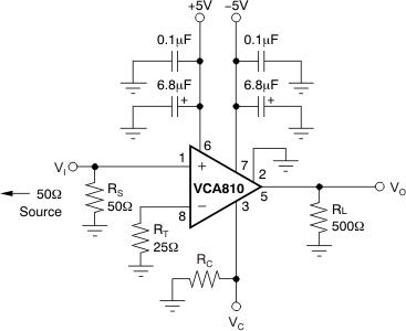
Figure 34 shows the circuit configuration used as the basis of the Electrical Characteristics and Typical Characteristics. Voltage swings reported in the specifications are taken directly at the input and output pins. For test purposes, the input impedance is set to 50 Ω with a resistance to ground. A 25-Ω resistance (RT) is included on the V− input to get bias current cancellation. Proper supply bypassing is shown in Figure 34, and consists of two capacitors on each supply pin: one large electrolytic capacitor (2.2 μF to 6.8 μF), effective at lower frequencies, and one small ceramic capacitor (0.1 μF) for high-frequency decoupling.
Notice that both inverting and noninverting inputs are connected to ground with a resistor (RS and RT). Matching the DC source impedance looking out of each input will minimize input offset voltage error.
9.1.2 Range-Finding TGC Amplifier
The block diagram in Figure 35 illustrates the fundamental configuration common to pulse-echo range finding systems. A photodiode preamp provides an initial gain stage to the photodiode.
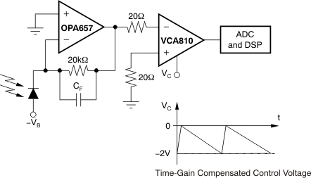 Figure 35. Typical Range-Finding Application
The control voltage VC varies the amplifier gain for a basic signal-processing requirement: compensation for distance attenuation effects, sometimes called time-gain compensation (TGC). Time-gain compensation increases the amplifier gain as the signal moves through the air to compensate for signal attenuation. For this purpose, a ramp signal applied to the VCA810 gain control input linearly increases the dB gain of the VCA810 with time.
9.1.3 Wide-Range AGC Amplifier
The voltage-controlled gain feature of the VCA810 makes this amplifier ideal for precision AGC applications with control ranges as large as 60 dB. The AGC circuit of Figure 36 adds an operational amplifier and diode for amplitude detection, a hold capacitor to store the control voltage and resistors R1 through R3 that determine attack and release times. Resistor R4 and capacitor CC phase-compensate the AGC feedback loop. The operational amplifier compares the positive peaks of output VO with a DC reference voltage, VR. Whenever a VO peak exceeds VR, the OPA820 output swings positive, forward-biasing the diode and charging the holding capacitor. This charge drives the capacitor voltage in a positive direction, reducing the amplifier gain. R3 and the CH largely determine the attack time of this AGC correction. Between gain corrections, resistor R1 charges the capacitor in a negative direction, increasing the amplifier gain. R1, R2, and CH determine the release time of this action. Resistor R2 forms a voltage divider with R1, limiting the maximum negative voltage developed on CH. This limit prevents input overload of the VCA810 gain control circuit.
Figure 37 shows the AGC response for the values shown in Figure 36.
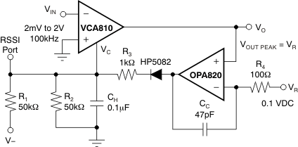 Figure 36. 60-dB Input Range AGC
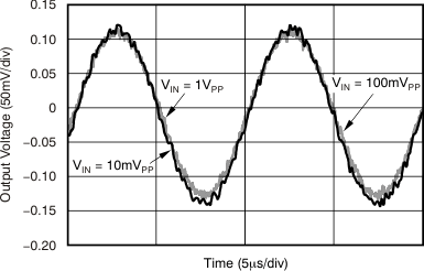 Figure 37. AGC Output Voltage for 100-kHz Sinewave at 10 mVPP, 100 mVPP, and 1 VPP
9.1.4 Stabilized Wein-Bridge Oscillator
Adding Wein-bridge feedback to the above AGC amplifier produces an amplitude-stabilized oscillator. As Figure 38 shows, this alternative requires the addition of just two resistors (RW1, RW2) and two capacitors
(CW1, CW2).
Connecting the feedback network to the amplifier noninverting input introduces positive feedback to induce oscillation. The feedback factor displays a frequency dependence due to the changing impedances of the CW capacitors. As frequency increases, the decreasing impedance of the CW2 capacitor increases the feedback factor. Simultaneously, the decreasing impedance of the CW1 capacitor decreases this factor. Analysis shows that the maximum factor occurs at  Hz, making this the frequency most conducive to oscillation. At this frequency, the impedance magnitude of CW equals RW, and inspection of the circuit shows that this condition produces a feedback factor of 1/3. Thus, self-sustaining oscillation requires a gain of three through the amplifier. The AGC circuitry establishes this gain level. Following initial circuit turn-on, R1 begins charging CH negative, increasing the amplifier gain from its minimum. When this gain reaches three, oscillation begins at fW; the continued charging effect of R1 makes the oscillation amplitude grow. This growth continues until that amplitude reaches a peak value equal to VR. Then, the AGC circuit counteracts the R1 effect, controlling the peak amplitude at VR by holding the amplifier gain at a level of three. Making VR an AC signal, rather than a DC reference, produces amplitude modulation of the oscillator output.
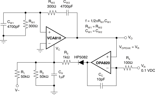 Figure 38. Amplitude-Stabilized Oscillator
9.1.5 Low-Drift Wideband Log Amplifier
The VCA810 can be used to provide a 2.5-MHz (–3 dB) log amp with low offset voltage and low gain drift. The exponential gain-control characteristic of the VCA810 permits simple generation of a temperature-compensated logarithmic response. Enclosing the exponential function in an op-amp feedback path inverts this function, producing the log response. Figure 39 shows the practical implementation of this technique. A DC reference voltage, VR, sets the VCA810 inverting input voltage. This configuration makes the amplifier output voltage
VOA = −GVR, where  .
.
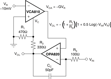 Figure 39. Temperature-Compensated Log Response
A second input voltage also influences VOA through control of gain G. The feedback operational amplifier forces VOA to equal the input voltage VIN connected at the operational amplifier inverting input. Any difference between these two signals drops across R3, producing a feedback current that charges CC. The resulting change in VOL adjusts the gain of the VCA810 to change VOA.
At equilibrium:

The operational amplifier forces this equality by supplying the gain control voltage,  .
.
Combining the last two expressions and solving for VOL yields the circuit’s logarithmic response:

An examination of this result illustrates several circuit characteristics. First, the argument of the log term, −VIN/VR, reveals an option and a constraint. In Figure 39, VR represents a DC reference voltage. Optionally, making this voltage a second signal produces log-ratio operation. Either way, the log term’s argument constrains the polarities of VR and VIN. These two voltages must be of opposite polarities to ensure a positive argument. This polarity combination results when VR connects to the inverting input of the VCA810. Alternately, switching VR to the amplifier noninverting input removes the minus sign of the log term argument. Then, both voltages must be of the same polarity in order to produce a positive argument. In either case, the positive polarity requirement of the argument restricts VIN to a unipolar range. Figure 40 illustrates these constraints.
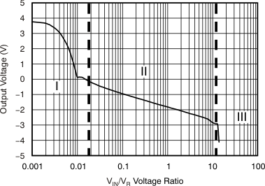 Figure 40. Test Result for LOG Amp for VR = −100 mV
The above VOL expression reflects a circuit gain introduced by the presence of R1 and R2. This feature adds a convenient scaling control to the circuit. However, a practical matter sets a minimum level for this gain. The voltage divider formed by R1 and R2 attenuates the voltage supplied to the VC terminal by the operational amplifier. This attenuation must be great enough to prevent any possibility of an overload voltage at the VC terminal. Such an overload saturates the VCA810 gain-control circuitry, reducing the amplifier’s gain. For the feedback connection of Figure 39, this overload condition permits a circuit latch. To prevent this, choose R1 and R2 to ensure that the operational amplifier cannot possibly deliver a more negative input than −2.5 V to the VC terminal.
Figure 40 exhibits three zones of operation described below:
Zone I: VC > 0 V. The VCA810 is operating in full attenuation (−80 dB). The noninverting input of the OPA820 will see ∼0 V. VOL is going to be the integration of the input signal.
Zone II: −2 V < VC < 0 V. The VCA810 is in its normal operating mode, creating the log relationship in Equation 7.
Zone III: VC < −2 V. The VCA810 control pin is out of range, and some measure should be taken so that it does not exceed –2.5 V. A limiting action could be achieved by using a voltage limiting amplifier.
9.1.6 Voltage-Controlled Low-Pass Filter
In the circuit of Figure 41, the VCA810 serves as the variable-gain element of a voltage-controlled low-pass filter. This section discusses how this implementation expands the circuit voltage swing capability over that normally achieved with the equivalent multiplier implementation. The circuit response pole responds to control voltage VC, according to the relationship in Equation 8:

where
With the components shown, the circuit provides a linear variation of the low-pass cutoff from 300 Hz to 1 MHz.
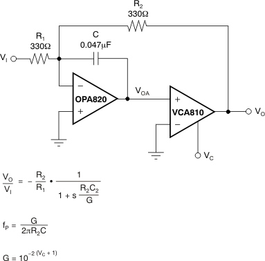 Figure 41. Tunable Low-Pass Filter
The response control results from amplification of the feedback voltage applied to R2. First, consider the case where the VCA810 produces G = 1. Then, the circuit performs as if this amplifier were replaced by a short circuit. Visually doing so leaves a simple voltage amplifier with a feedback resistor bypassed by a capacitor. This basic circuit produces a response pole at  .
.
For G > 1, the circuit applies a greater voltage to R2, increasing the feedback current this resistor supplies to the summing junction of the OPA820. The increased feedback current produces the same result as if R2 had been decreased in value in the basic circuit described above. Decreasing the effective R2 resistance moves the circuit pole to a higher frequency, producing the  response control.
Finite loop gain and a signal-swing limitation set performance boundaries for the circuit. Both limitations occur when the VCA810 attenuates, rather than amplifies, the feedback signal. These two limitations reduce the circuit’s utility at the lower extreme of the VCA810 gain range. For −1 ≤ VC ≤ 0, this amplifier produces attenuating gains in the range from 0 dB to −40 dB. This range directly reduces the net gain in the circuit’s feedback loop, increasing gain error effects. Additionally, this attenuation transfers an output swing limitation from the OPA820 output to the overall circuit’s output. Note that OPA820 output voltage, VOA, relates to VO through the expression, VO = G × VOA. Thus, a G < 1 limits the maximum VO swing to a value less than the maximum VOA swing.
Figure 42 shows the low-pass frequency for different control voltages.
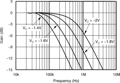 Figure 42. Voltage-Controlled Low-Pass Filter Frequency Response
9.1.7 Tunable Equalizer
A circuit analogous to the above low-pass filter produces a voltage-controlled equalizer response. The gain control provided by the VCA810 of Figure 43 varies this circuit response zero from 1 Hz to 10 kHz, according to the relationship of Equation 9:

To visualize the circuit’s operation, consider a circuit condition and an approximation that permit replacing the VCA810 and R3 with short circuits. First, consider the case where the VCA810 produces G = 1. Replacing this amplifier with a short circuit leaves the operation unchanged. In this shorted state, the circuit is simply a voltage amplifier with an R-C bypass around R1. The resistance of this bypass, R3, serves only to phase-compensate the circuit, and practical factors make R3 << R1. Neglecting R3 for the moment, the circuit becomes just a voltage amplifier with a capacitive bypass of R1. This circuit produces a response zero at  .
.
Adding the VCA810 as shown in Figure 43 permits amplification of the signal applied to capacitor C, and produces voltage control of the frequency fZ. Amplified signal voltage on C increases the signal current conducted by the capacitor to the operational amplifier feedback network. The result is the same as if C had been increased in value to GC. Replacing C with this effective capacitance value produces the circuit control expression  .
.
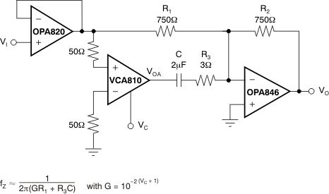 Figure 43. Tunable Equalizer
Another factor limits the high-frequency performance of the resulting high-pass filter: the finite bandwidth of the operational amplifier. This limits the frequency duration of the equalizer response. Limitations such as bandwidth and stability are clearly shown in Figure 44.
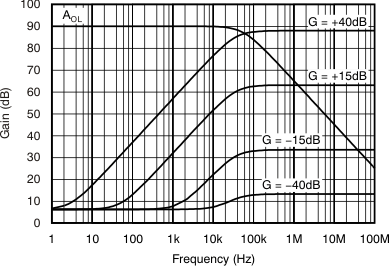 Figure 44. Amplifier Noise Gain and AOL for Different Gain
Other limitations of this circuit are stability versus VCA810 gain and input signal level for the circuit. Figure 44 also illustrates these two factors. As the VCA810 gain increases, the crossover slope between the AOL curve of the OPA846 and noise gain will be greater than 20 dB/decade, rendering the circuit unstable. The signal level for high gain of the VCA810 will meet two limitations: the output voltage swings of both the VCA810 and the OPA846. The expression VOA = GVI relates these two voltages. Thus, an output voltage limit VOAL constrains the input voltage to VI ≤ VOAL/G.
With the components shown, BW = 50 kHz. This bandwidth provides an integrator response duration of four decades of frequency for fZ = 1 Hz, dropping to one decade for fZ = 10 kHz.
9.1.8 Voltage-Controlled Band-Pass filter
The variable gain of the VCA810 also provides voltage control over the center frequency of a band-pass filter. As shown in Figure 45, this filter follows from the state-variable configuration with the VCA810 replacing the inverter common to that configuration. Variation of the VCA810 gain moves the filter’s center frequency through a 100:1 range following the relationship of Equation 10:

As before, variable gain controls a circuit time constant to vary the filter response. The gain of the VCA810 amplifies or attenuates the signal driving the lower integrator of the circuit. This amplification alters the effective resistance of the integrator time constant, producing the response of Equation 11:

Evaluation of this response equation reveals a passband gain of AO = –1, a bandwidth of BW = 1/(2πRC), and a selectivity of  . Note that variation of control voltage VC alters Q but not bandwidth.
The gain provided by the VCA810 restricts the output swing of the filter. Output signal VO must be constrained to a level that does not drive the VCA810 output, VOA, into its saturation limit. Note that these two outputs have voltage swings related by VOA = GVO. Thus, a swing limit VOAL imposes a circuit output limit of VOL ≤ VOAL/G.
See Figure 46 for the frequency response for two different gain conditions of the schematic shown in Figure 45. In particular, notice the center frequency shift and the selectivity of Q changing as the gain is increased.
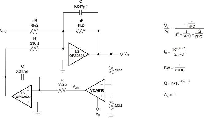 Figure 45. Tunable Band-Pass Filter
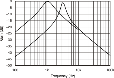 Figure 46. Tunable Band-Pass Filter Response
9.2 Typical Application
A common use of the log amplifier above involves signal compounding. The inverse function, signal expanding, requires an exponential transfer function. The VCA810 produces this latter response directly, as shown in Figure 47. DC reference VR again sets the amplifier input voltage, and the input signal VIN now drives the gain control point. Resistors R1 and R2 attenuate this drive to prevent overloading the gain control input. Setting these resistors at the same values as in the preceding log amp produces an exponential amplifier with the inverse function of the log amplifier.
Testing the circuit given in Figure 47 gives the exponential response shown in Figure 48.
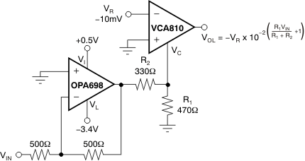 Figure 47. Exponential Amplifier
9.2.1 Design Requirements
To build a wide dynamic range wide exponential amplifier we need an amplifier with continuous voltage gain control, gain range over 40 dB, low noise, and high maximum gain. The VCA810 has ±40 dB of gain range, so it meets this criteria. It also has continuous voltage gain control and can support up to 100 V/V of voltage gain.
9.2.2 Detailed Design Procedure
An exponential amplifier will have a linear response on a logarithmic scale. The linear in dB gain control of the VCA810 is ideal for this application. Note that the input to this circuit is the gain control pin. Using the gain control pin as the input is what gives an exponential gain response. The design involves the use of an OPA698 to provide the proper DC bias voltage to the gain control pin on the VCA810. The OPA698 supply voltage was chosen based on the input voltage requirement of the VCA810. The reference voltage (VR) is used to set the DC output voltage. The reference voltage cannot be 0 V, but it must be small so that at maximum gain the amplifier outputs are not saturated. In Figure 47 design the reference voltage is set to –10 mV.
9.2.3 Application Curve
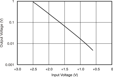 Figure 48. Exponential Amplifier Response
