JAJS366D October 2006 – October 2024 XTR111
PRODUCTION DATA
- 1
- 1 特長
- 2 アプリケーション
- 3 概要
- 4 Pin Configurations and Functions
- 5 Specifications
- 6 Detailed Description
- 7 Application and Implementation
- 8 Device and Documentation Support
- 9 Revision History
- 10Mechanical, Packaging, and Orderable Information
パッケージ・オプション
メカニカル・データ(パッケージ|ピン)
サーマルパッド・メカニカル・データ
発注情報
6.3.6 Voltage Regulator
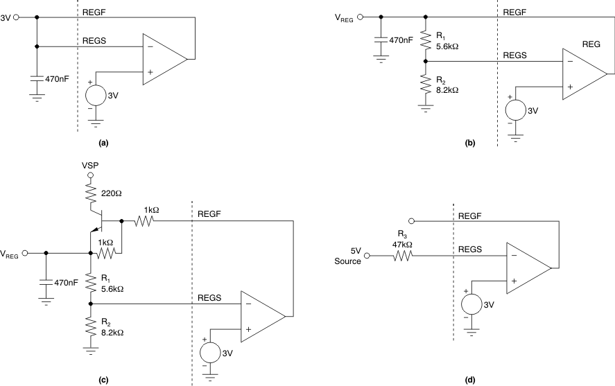
The externally adjustable voltage regulator provides up to 5mA of current and offers drive (REGF) and sense (REGS) to allow external setting of the output voltage. Figure 6-7 shows the voltage regulator basic connections. The sense input (REGS) is referenced to 3.0V representing the lowest adjustable voltage level. An external resistor divider sets VREGF.
 Figure 6-7 Basic Connections of the
Voltage Regulator
Figure 6-7 Basic Connections of the
Voltage RegulatorTable 6-2 provides example values for the regulator adjustment resistors.
| VREGF | R1 | R2 |
|---|---|---|
| 3V | 0kΩ | — |
| 3.3V | 3.3kΩ | 33kΩ |
| 5V | 5.6kΩ | 8.2kΩ |
| 12.4V | 27kΩ | 8.6kΩ |
The voltage at REGF is limited by the supply voltage. If the supply voltage drops close to the set voltage, the driver output saturates and follows the supply with a voltage drop of less than 1V (depending on load current and temperature).
For good stability and transient response, use a load capacitance of 470nF or greater. The bias current into the sense input (REGS) is typically less than 1μA. Consider the bias current when selecting high resistance values for the voltage setting because the bias current lowers the voltage and produces additional temperature dependence.
The REGF output cannot sink current. In case of supply-voltage loss, the output is protected against the discharge currents from load capacitors by internal protection diodes; the peak current must not exceed 25mA.
If the voltage regulator output is not used, connect REGF to REGS (3V mode) loaded with a 2.2nF capacitor. Alternatively, overdrive the loop pulling REGS high; Figure 6-7d shows this method.