JAJS366D October   2006  – October 2024 XTR111

PRODUCTION DATA  

  1.   1
  2. 特長
  3. アプリケーション
  4. 概要
  5. Pin Configurations and Functions
  6. Specifications
    1. 5.1 Absolute Maximum Ratings
    2. 5.2 ESD Ratings
    3. 5.3 Recommended Operating Conditions
    4. 5.4 Thermal Information
    5. 5.5 Electrical Characteristics
    6. 5.6 Typical Characteristics
  7. Detailed Description
    1. 6.1 Overview
    2. 6.2 Functional Block Diagram
    3. 6.3 Feature Description
      1. 6.3.1 Explanation of Pin Functions
      2. 6.3.2 Dynamic Performance
      3. 6.3.3 External Current Limit
      4. 6.3.4 External MOSFET
      5. 6.3.5 Output Error Flag and Disable Input
      6. 6.3.6 Voltage Regulator
      7. 6.3.7 Level Shift of 0V Input and Transconductance Trim
    4. 6.4 Device Functional Modes
  8. Application and Implementation
    1. 7.1 Application Information
      1. 7.1.1 Input Voltage
      2. 7.1.2 Error Flag Delay
      3. 7.1.3 Voltage Output Configuration
      4. 7.1.4 4mA-to-20mA Output
    2. 7.2 Typical Applications
      1. 7.2.1 0mA–20mA Voltage-to-Current Converter
        1. 7.2.1.1 Design Requirements
        2. 7.2.1.2 Detailed Design Procedure
        3. 7.2.1.3 Application Curve
      2. 7.2.2 Additional Applications
    3. 7.3 Power Supply Recommendations
    4. 7.4 Layout
      1. 7.4.1 Layout Guidelines
        1. 7.4.1.1 Package and Heat Dissipation
        2. 7.4.1.2 Thermal Pad Guidelines
      2. 7.4.2 Layout Example
  9. Device and Documentation Support
    1. 8.1 Device Support
      1. 8.1.1 サード・パーティ製品に関する免責事項
    2. 8.2 Documentation Support
      1. 8.2.1 Related Documentation
    3. 8.3 ドキュメントの更新通知を受け取る方法
    4. 8.4 サポート・リソース
    5. 8.5 Trademarks
    6. 8.6 静電気放電に関する注意事項
    7. 8.7 用語集
  10. Revision History
  11. 10Mechanical, Packaging, and Orderable Information

パッケージ・オプション

メカニカル・データ(パッケージ|ピン)
サーマルパッド・メカニカル・データ
発注情報

4mA-to-20mA Output

The XTR111 does not provide internal circuits to generate 4mA with 0V input signal. Figure 7-3 shows that the most common way to shift the input signal is a two-resistor network connected to a voltage reference and the signal source. This arrangement allows easy adjustment for overrange and underrange conditions. The example assumes a 5V reference (VREF) that equals the full-scale signal voltage and a signal span of 0V to 5V for 4mA-to-20mA (IMIN to IMAX) output.

The voltage regulator output or a more precise reference can be used as VREF. Observe the potential drift added by the drift of the resistors and the voltage reference.
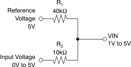
XTR111 Resistive
                    Divider for IMIN-to-IMAX Output (4mA to 20mA) With 0V to
                        VFS Signal Source Figure 7-3 Resistive Divider for IMIN-to-IMAX Output (4mA to 20mA) With 0V to VFS Signal Source