-
DAC101C08xx 10-Bit Micro Power Digital-to-Analog Converter With an I2C-Compatible Interface SNVS801B April 2012 – January 2016 DAC101C081 , DAC101C081Q , DAC101C085
PRODUCTION DATA.
-
DAC101C08xx 10-Bit Micro Power Digital-to-Analog Converter With an I2C-Compatible Interface
- 1 Features
- 2 Applications
- 3 Description
- 4 Revision History
- 5 Description (continued)
- 6 Device Comparison Table
- 7 Pin Configuration and Functions
- 8 Specifications
- 9 Detailed Description
- 10Application and Implementation
- 11Power Supply Recommendations
- 12Layout
- 13Device and Documentation Support
- 14Mechanical, Packaging, and Orderable Information
- IMPORTANT NOTICE
パッケージ・オプション
メカニカル・データ(パッケージ|ピン)
サーマルパッド・メカニカル・データ
発注情報
DAC101C08xx 10-Bit Micro Power Digital-to-Analog Converter With an I2C-Compatible Interface
1 Features
- Ensured Monotonicity to 10-bits
- Low Power Operation: 156-µA maximum at 3.3 V
- Extended Power Supply Range (2.7 V to 5.5 V)
- I2C-Compatible 2-Wire Interface Which Supports Standard (100-kHz), Fast (400-kHz), and High-Speed (3.4-MHz) Modes
- Rail-to-Rail Voltage Output
- Very Small Package
- DAC101C081Q is AEC Q100 Grade 1 Qualified and Manufactured on Automotive Grade Flow
- Resolution: 10 Bits
- INL: ±2 LSB (Maximum)
- DNL: +0.3/-0.2 LSB (Maximum)
- Setting Time: 6-µs (Maximum)
- Zero Code Error: +10-mV (Maximum)
- Full-Scale Error: −0.7 %FS (Maximum)
- Supply Power (Normal): 380-µW (3-V) / 730-µW (5-V) Typical
- Supply Power (Power Down): 0.5-µW (3-V) / 0.9-µW (5-V) Typical
2 Applications
- Industrial Process Control
- Portable Instruments
- Digital Gain and Offset Adjustment
- Programmable Voltage and Current Sources
- Test Equipment
- Automotive
3 Description
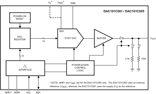
The DAC101C081 device is a 10-bit, single channel, voltage-output digital-to-analog converter (DAC) that operates from a 2.7 V to 5.5 V supply. The output amplifier allows rail-to-rail output swing and has an 6-µsec settling time. The DAC101C081 uses the supply voltage as the reference to provide the widest dynamic output range and typically consumes 132 µA while operating at 5.0 V. It is available in 6-lead SOT and WSON packages and provides three address options (pin selectable).
As an alternative, the DAC101C085 provides nine I2C™ addressing options and uses an external reference. It has the same performance and settling time as the DAC101C081 and is available in an 8-lead VSSOP.
The DAC101C081 and DAC101C085 use a 2-wire, I2C-compatible serial interface that operates in all three speed modes, including high speed mode (3.4 MHz). An external address selection pin allows up to three DAC101C081 or nine DAC101C085 devices per 2-wire bus. Pin compatible alternatives to the DAC101C081 are available that provide additional address options.
Device Information(1)
| PART NUMBER | PACKAGE | BODY SIZE (NOM) |
|---|---|---|
| DAC101C081 | WSON (6) | 2.20 mm × 2.50 mm |
| SOT (6) | 1.60 mm × 2.90 mm | |
| DAC101C085 | VSSOP (8) | 3.00 mm × 3.00 mm |
| DAC101C081Q | WSON (6) | 2.20 mm × 2.50 mm |
- For all available packages, see the orderable addendum at the end of the data sheet.
Block Diagram

4 Revision History
Changes from A Revision (March 2013) to B Revision
- Added ESD Ratings table, Feature Description section, Device Functional Modes, Application and Implementation section, Power Supply Recommendations section, Layout section, Device and Documentation Support section, and Mechanical, Packaging, and Orderable Information section. Go
- Added addresses that the DAC responds to on the I2C bus.Go
Changes from * Revision (March 2013) to A Revision
- Changed layout of National Data Sheet to TI formatGo
5 Description (continued)
The DAC101C081 and DAC101C085 each have a 16-bit register that controls the mode of operation, the power-down condition, and the output voltage. A power-on reset circuit ensures that the DAC output powers up to zero volts. A power-down feature reduces power consumption to less than a microWatt. Their low power consumption and small packages make these DACs an excellent choice for use in battery operated equipment. Each DAC operates over the extended industrial temperature range of −40°C to +125°C.
The DAC101C081 and DAC101C085 are each part of a family of pin compatible DACs that also provide 12 and 8 bit resolution. For 12-bit DACs see the DAC121C081 and DAC121C085. For 8-bit DACs see the DAC081C081 and DAC081C085.